( ESNUG 485 Item 5 ) -------------------------------------------- [06/08/10]
Subject: (ESNUG 470 #1) 100X compression, Talus Design, Mentor Tessent
> Owning DEF means they can use DFT MAX or TestKompress easily. From a PD
> view, Mentor owns TestKompress but Sierra is still a raw tool, hence
> they're #3. Magma has no compression and I don't know if they can even
> support DFT MAX nor TestKompress. Atoptech a newbie here.
>
> - Jonathan Bahl
> COT Consulting, Inc. Toronto, Canada
From: Debo Sekoni <dsekoni=user domain=altasens not mom>
Hi, John,
We evaled Magma's Talus Design and Mentor's Tessent TestKompress to see if
it can really get a 100X scan compression (as the vendors claim.) Our task
for our 2.6 million gate RTL design was to:
1. Insert scan logic.
2. Insert compression logic and connected it to the scan logic.
3. Create and have verified scan patterns.
The first step, before jumping straight in, was to do a design requirement
exercise. That is, take a look at the register transfer level (RTL) design
and determine what it will take to insert scan logic into it. This may
require you to synthesize the RTL design into a gate netlist. Ask yourself
the following questions:
a. Will the design be laid out as a single block (top-down) or multiple
blocks pieced together at the chip level (bottom-up)?
b. How many input/output (I/O) pins are available for scan enable, scan
clock, scan reset/set, scan input, and scan output?
c. Are there any I/O pins left for the scan compression clock and update?
d. How many clock groups are in the design?
e. Are the clocks and resets active-high or active-low?
f. Is there third-party Intellectual Property (IP) blocks in your RTL
design?
g. What is my compression target?
By default, both tools use a top-down DFT flow; that is, you define the DFT
constraints on the top level of your design (whether its flattened or
hierarchical). Using the top-level DFT constraints, Talus Design performs
DFT design rule checking (DRC), auto repair of DFT DRC violations, and scan
insertion on the entire design. Under some circumstances, however, you
might need to use a bottom-up flow if the design contains a third-party
block with scan logic.
Similarly, Mentor's Tessent uses top-level DFT constraints to create and
insert the Embedded Deterministic Test (EDT) logic block. EDT is the
technology used by TestKompress to provide compression of scan test data and
reduction in test time. To learn more about EDT, see the Mentor Graphics
Tessent TestKompress documentation.
About the Design
================
The design referenced in this email is a mixed-signal System-on-Chip (SoC)
(Figure 1). The SoC contains one analog core, one I/O pad ring and two
identical digital core blocks, which are also called "hemispheres." One
hemisphere is designated "NORTH" and the other is "SOUTH." Each hemisphere
contains 1.3 million gates, of which roughly 57,300 (57K) gates are non-scan
registers (flip-flops). Each hemisphere also has two dedicated scan outputs
and a dedicated internal testmode register. Both hemispheres share the same
scan input, scan clock, scan reset, and scan enable with functional I/O
signals. The internal architecture of the mixed-signal SoC interfaces with
the outside world through the I/O pad ring. The entire digital core is
treated as a single block, using the Talus Design top-down flow without any
I/O pads. No scan information is contained in the RTL-level design. The
digital core is duplicated twice during final full chip finishing. The two
hemispheres are differentiated by a single bit, 0 for the South hemisphere
and 1 for the North hemisphere.
At this point, let's review the design:
a. The entire digital core is treated as a single block and processed only
once within the Talus Physical Design top-down flow, including scan
logic insertion.
b. The entire digital core is duplicated twice during final full chip
finishing, differentiated by a single bit: 0 for South and 1 for North.
c. Each hemisphere in the full chip has two dedicated scan outputs,
DIGTEST1 and DIGTEST2, to monitor the stimuli response.
d. Each hemisphere in the full chip has a dedicated internal testmode
flip-flop to put the SoC in scan test mode.
e. Each hemisphere in the full chip shares the scan clock, scan input,
scan reset, and scan enable from the I/O pad ring to apply the stimuli.
f. Each hemisphere in the full chip shares the scan compression clock and
update signals from the I/O pad ring to control the compression logic.
g. No scan information is contained in the RTL-level digital design.
h. Each hemisphere has roughly 57K gates that are non-scan flip-flops, for
a total of 114K non-scan flip-flops.
i. The two hemispheres do not communicate with each other in the full chip.
Figure 1 shows block-level diagram representing the full chip SoC.
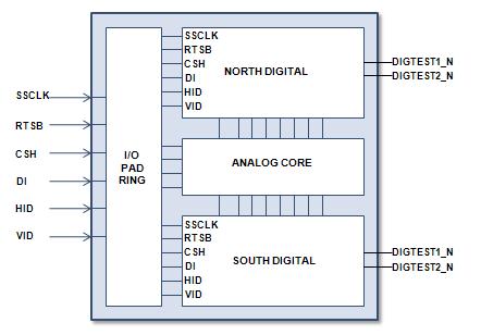 Figure 1. Full chip SoC
Before you begin, be sure you have prepared the Volcano database for your
libraries. For more information about creating a Volcano database, see the
Magma Talus Design documentation. The first time you follow this procedure,
you will probably run the commands interactively. Once you determine a
successful combination, you can add the commands to a Tool Command Language
(TCL) script file to run automatically. Once the design is complete, you
can create the list of commands to run your DFT program.
The following sections describe the major steps in the process:
A. Inserting Scan Logic for Compression
B. Inserting Scan Compression
C. Running ATPG for Scan Compression
D. Conclusion
Inserting Scan Logic for Compression
====================================
As mentioned earlier, we assume that the reader is familiar with the two
types of physical design flows: top-down and bottom-up. The benefit of one
flow over the other is determined by your design requirements. For more
information about physical design flows, see the Magma Talus Design docs.
For this email, the Talus Design Flat flow is used.
We begin with a synthesized Volcano database, that is, the RTL design has
been elaborated and synthesized into a gate netlist. Our first task is to
create a compression.tcl file, then add the commands described in the
following tasks to the compression.tcl file:
1. Define I/O pins for scan compression DFT architecture.
2. Configure I/O pins for scan compression DFT architecture.
3. Define scan chains for scan compression DFT architecture.
4. Define flip-flops to be excluded from scan logic insertion.
5. Identify automatic DFT repair functions to enable by running
pre-scan DFT design rule checks (DRC).
6. Enable automatic DFT repair functions.
7. Configure scan chain mixing.
8. Re-run pre-scan DFT DRC.
9. Insert scan logic for scan compression.
10. Run post-scan DFT DRC.
11. Review pre-scan and post-scan DFT DRCs.
These steps are described below in detail.
1. Define the scan compression I/O pin configuration for ease of use during
the scan logic insertion process by specifying the following variables:
set $m /dig_top/dig_top (where m is set to the top level module
name)
set scan_clock $m/mpin:SCCLK
set scan_input $m/mpin:DI
set scan_enable $m/mpin:CSH
set scan_reset $m/mpin:RSTB
set scan_output $m/mpin:DIGTEST1
set scan_mode $m/scan_mode_enable_reg/pin:Q
set edt_clock $m/mpin:VID
set edt_update $m/mpin:HID
These variables will be used by almost every Talus Design command. It
is important to define these variables early in the flow.
2. Using the I/O pin configuration, define the following top-level DFT pin
constraints to ensure proper operation during scan testing:
a. Define scan clocks:
force dft scan clock $m $scan_clock -active high
b. Define scan mode control and constraint:
force dft scan control $m $scan_mode test_mode -active high
force dft setup constraint $m $scan_mode 1 shift
force dft setup constraint $m $scan_mode 1 capture
c. Define scan enable control and constraint:
force dft scan control $m $scan_enable scan_enable -active high
force dft setup constraint $m $scan_enable 1 shift
force dft setup constraint $m $scan_enable 0 capture
d. Define scan reset/set constraint:
force dft setup constraint $m $scan_reset 1 shift
force dft setup constraint $m $scan_reset 1 capture
3. Define the scan chains for scan compression DFT architecture.
When defining the scan chains for scan compression, the target
compression ratio determines how many scan chains are required per scan
channel to achieve compression. In this example, we have specified one
scan channel, because this is what we have available and we desire one
hundred compression ratio (100x). Therefore, the command to configure
a one hundred compression ratio to one scan channel (1:1:100) is:
for { set i 0 } { $i < 100 } {incr i}
{
force dft scan chain $m $i SI_$i SO_$i
// where: SI_$i and SO_$i are the scan
// input/output pins to be used for
// the internal scan chains
}
Talus Design will use the configuration above to insert 100 scan chains,
each chain equal to the total number of non-scan flip-flops minus the
total number of excluded flip-flops divided by 100. Below is an example:
Chain0 == SI_0 | SO_0 == (57279 - 39)/100 == 573 flip-flops
Chain1 == SI_1 | SO_1 == (57279 - 39)/100 == 573 flip-flops
...
Chain99 == SI_99 | SO_99 == (57279 - 39)/100 == 572 flip-flops
Defining scan chains...
MSG-10 While running 'force dft scan chain
/work/iso_dig_top/iso_dig_top 0 SI_0 SO_0':
DFT-625 WARNING: The scan input pin 'SI_0' does not exist. The pin
'SI_0' will be created during scan insertion.
DFT-625 WARNING: The scan output pin 'SO_0' does not exist. The pin
'SO_0' will be created during scan insertion.
MSG-10 While running 'force dft scan chain
/work/iso_dig_top/iso_dig_top 1 SI_1 SO_1':
...
The scan chain configuration above is referred to as "one scan input
to one scan output channel, 100x compression ratio," or (1:1:100).
4. Specify the flip-flops to be excluded from scan logic insertion. For
example, it is necessary to exclude the scan mode flip-flop from scan
logic insertion to prevent the scan mode flip-flop from changing to a
disabled state (1 to 0):
force dft setup disable $m $scan_mode
For this design, 39 flip-flops are excluded from scan logic insertion.
5. Identify automatic DFT repair functions to enable by running pre-scan
DFT design rule checks (DRC).
run dft check $m $l -pre_scan
The following example shows the pre-scan DFT DRC report that resulted
from running the pre-scan "run dft check" command:
DTC-100 DRC rules checked on this circuit
NDTC-1
NDTC-1 Pre-scan DRC status:
NDTC-1 - CLK: FAIL (57099 violation(s))
NDTC-1 - CLK-1: FAIL (57082 failure(s))
NDTC-1 - CLK-2: FAIL (9 failure(s))
NDTC-1 + CLK-13: pass (8 warning(s))
NDTC-1 - RST: FAIL (114534 violation(s))
NDTC-1 - RST-1: FAIL (57237 failure(s))
NDTC-1 + RST-2: pass (57237 warning(s))
NDTC-1 + RST-5: pass (30 warning(s))
NDTC-1 + RST-6: pass (30 note(s))
NDTC-1 + LAT: pass (2655 violation(s))
NDTC-1 + LAT-1: pass (2655 warning(s))
NDTC-1 + BUS: pass (0 violation(s))
NDTC-1 + CFL: pass (0 violation(s))
NDTC-1 + DSN: pass (15 violation(s))
NDTC-1 + DSN-1: pass (11 note(s))
NDTC-1 + DSN-2: pass (4 note(s))
NDTC-1
NDTC-1 ("FAIL" means that violations of severity failure have been
detected)
NDTC-1 ("pass" means that no failure has been detected, but there
might be violations of severity warning or note reported)
NDTC-1 (for more details, run "report dft rule violation")
In the DFT DRC, Talus Design attaches a severity level to each violation
it finds. Details and description of the different rules can be found
in the result from the "report dft rule violation."
The pre-scan DFT DRC report (from the example above) is telling us:
a. Violations exist for the scan clock specified, because the internal
clock pin of flip-flops in the design is not controllable from the
top-level SCCLK ($scan_clock) port defined. Since the original RTL
design contained no scan information, scan clock violations should
be expected in the pre-scan DFT DRC.
b. Violations exist for the scan reset specified, because the internal
reset pin of flip-flops in the design are not controllable from the
top-level RSTB ($scan_reset) port. This means we will need to
specify a "config dft repair" command to repair the reset and clock.
c. There are 2655 passing warnings for the transparency of latches
(LAT).
d. No violations exist for combinational feedback loops (CFL).
6. Enable the following "force dft repair" commands, as needed to perform
automatic DFT repair during scan logic insertion:
a. To repair the clock:
force dft repair clock_violation $m $scan_mode -manual $scan_clock
b. To repair the reset:
force dft repair reset_violation $m $scan_mode
c. To repair the latch:
force dft repair latch $m $scan_enable
(optional for this design example)
d. To repair combinational feedback:
force dft repair combo_loop $m $scan_mode $scan_clock
(optional for this design example)
7. Configure scan chain mixing of flip-flops in a scan chain.
config dft scan chain_mix clock on
config dft scan chain_mix edge on
The "config dft scan chain_mix" command configures the mixing of flip-
flops in a scan chain. By default, only the flip-flops in the same
clock domain and having the same clock edge can reside in the same scan
chain. However, to balance the length of scan chains, it is often
necessary to mix the flip-flops in different clock domains or with
different clock edges in the same scan chain. This command specifies
the allowed method for mixing flip-flops in a scan chain.
Since we have specified only one scan clock, we need not worry about
mixing clocks and edges. We can expect our scan chains to be balanced.
For designs with multiple clock domains and edges, performing the design
requirement exercise helps to reduce multiple iterations before the scan
logic is actually inserted.
8. Insert scan logic for scan compression.
run dft scan insert $m $l
Talus Design will automatically repair all DFT DRC violations, replace
all the flip-flops in the design to scan flip-flops, and connect all the
scan flip-flops across 100 scan chains, evenly balanced.
Below is an example of the scan logic insertion for scan compression.
INS-369 Preparing repair of DFT rule violations...
INS-200 Repairing reset rule violations...
INS-369 Repairing clock rule violations...
INS-369 Updating design data at volcano...
INS-369 END of DFT repair.
INS-380 39 flip-flops are disabled by 'force dft setup disable ...'
command.
INS-369 Processing Scan Insertion Information...
INS-743 DFT clock '/work/dig_top/dig_top/mpin:SCCLK'(Return-To-0:
57240 flop(s) at leading edge
INS-200 Begin of scan chain information
INS-692 Number of scan chains = 100
INS-200 End of scan chain information
INS-621 Identifying Lock-up latches...
INS-408 No lock-up latches are required for your design.
INS-369 Replacing flip-flops by scan cells...
INS-369 Routing Scan Paths...
DFT-123 Assigning scan chain blocks for reordering ...
DFT-123 Saving the scan trace information ...
DFT-111 Chain id 0 consists of 1 block with 573 length
(573 reorderable )
DFT-111 Chain id 1 consists of 1 block with 573 length
(573 reorderable )
DFT-111 Chain id 2 consists of 1 block with 573 length
(573 reorderable )
DFT-111 Chain id 3 consists of 1 block with 573 length
(573 reorderable )
...
DFT-111 Chain id 98 consists of 1 block with 572 length
(572 reorderable )
DFT-111 Chain id 99 consists of 1 block with 572 length
(572 reorderable )
DFT-110 End of Scan Tracing.
9. Run post-scan DFT DRC.
run dft check $m $l -post_scan
There should be no violations (FAILs) in the post-scan DFT DRC report.
Its verification of scan-chain integrity is shown below:
NDTC-1 Post-scan DRC status:
NDTC-1 + CLK: pass (2 violation(s))
NDTC-1 + CLK-5: pass (1 warning(s))
NDTC-1 + CLK-8: pass (1 warning(s))
NDTC-1 + RST: pass (0 violation(s))
NDTC-1 + LAT: pass (2655 violation(s))
NDTC-1 + LAT-1: pass (2655 warning(s))
NDTC-1 + BUS: pass (0 violation(s))
NDTC-1 + CFL: pass (0 violation(s))
NDTC-1 + DSN: pass (14 violation(s))
NDTC-1 + DSN-1: pass (11 note(s))
NDTC-1 + DSN-2: pass (3 note(s))
NDTC-1 + TSC: pass (0 violation(s))
NDTC-1
NDTC-1 ("FAIL" means that violations of severity failure have been
detected)
NDTC-1 ("pass" means that no failure has been detected, but there
might be violations of severity warning or note reported)
NDTC-1 (for more details, run "report dft rule violation")
DTC-6014 warning: Passing all scan and DFT rules may not guarantee
that this design is ready for ATPG (automatic test
pattern generation) and proper scan testing
operation. Please refer to the message(s)
DTC-2037, DTC-2033, and DTC-2036 (not shown here).
10. Review pre-scan and post-scan DFT DRC.
Earlier, the pre-scan DFT DRC report told us:
1. Violations existed for the scan clock specified, because the
internal clock pin of flip-flops in the design is not controllable
from the top-level SCCLK ($scan_clock) port defined.
2. Violations existed for the scan reset specified, because the
internal reset pin of flip-flops in the design are not controllable
from the top-level RSTB ($scan_reset) port.
3. There were 2655 passing warnings for the transparency of latches
(LAT).
4. No violations exist for combinational feedback loops (CFL).
Now, the post-scan DFT DRC report is telling us:
1. There are two passing warnings for the scan clock specified.
2. No violations exist for the scan reset specified (RST).
3. There are 2655 passing warnings for the transparency of latches
(LAT).
4. No violations exist for combinational feedback loops (CFL).
Since no FAILs have been reported, there are no issues on the design
that will prevent the insertion of scan compression EDT logic, and
subsequently ATPG.
Inserting Scan Compression
==========================
The next task is to insert EDT logic into the design and connect the EDT
logic to the defined scan channel input and output I/O ports. The "fix
dft tk" command performs the following actions:
a. Calls the third-party test compression tool, Mentor Graphics
Tessent TestKompress.
b. Generates the EDT logic.
c. Synthesizes the EDT logic.
d. Connects the scan chains to the EDT logic.
e. Integrates the EDT logic into the top-level.
The final product is a gate netlist with the following DFT architecture:
- 1 scan input.
- 1 scan output.
- 1 scan clock.
- 1 scan reset.
- 1 scan enable.
- 1 edt_clock.
- 1 edt_update.
- 1 internal test mode flip-flop
- 100 internal scan chains.
The "fix dft tk" command uses a series of set commands to specify the option
settings for the EDT logic. Add the commands described in the following
tasks to the compression.tcl file:
1. Set the scan model.
2. Set the base name for the EDT logic block.
3. Set the instance name for the EDT logic block.
4. Set the paired list of {name connection_point} for the EDT channel
inputs.
5. Set the paired list of {name connection_point} for the EDT channel
outputs.
6. Set the paired list of {name connection_point} for the EDT_CLOCK
signal.
7. Set the paired list of {name connection_point} for the EDT_UPDATE
signal.
8. Set the paired list of {name connection_point} for the EDT_SELECT
signal.
9. Set the paired list of {name connection_point} for the EDT BYPASS
signal.
10. Set the paired list of {name connection_point} for the shift enable
signal.
11. Set hierarchical preference. Specify 1 to create a new hierarchy.
Specify 0 to maintain the flat hierarchy.
12. Set edt_bypass preference. Specify 1 if edt_bypass is to be
included in the design. Specify 0 to exclude.
13. Set lockup latch preference. Specify 1 if lockup latches need to be
created inside the EDT block. Specify 0 to exclude.
14. Set addmux preference. Specify 1 if the EDT channel output(s)
is(are) shared with functional I/O pins, and MUXes are not already
inserted to share the signal. Specify 0 if MUXes are already
inserted to share the signal.
15. Set addgate preference. Specify 1 if the EDT channel input(s)
is(are) shared with functional pins, and you want to gate off the
signals to the EDT block when not in EDT mode.
16. Set scan chain range preference. A paired list of either absolute
numbers (for example, {300 350}) or relative numbers (for example,
{-10 +30}), specifying the longest chain range for EDT generation.
See the Mentor Graphics Tessent TestKompress documentation for
details.
17. Set tk_call: A string to invoke the test compression tool
Below is the series of set commands specified for our design:
puts "###########################################################"
puts "##### Setting SCAN COMPRESSION constraints #####"
puts "###########################################################"
set scanmodel $m
set edtbase dig_top
set edtinst ${edtbase}_edt_inst
puts "###########################################################"
set edt_input [list DI $m/pad_SI_BUFFER/pin:Z ]
set edt_output [list DIGTEST1 $m/pad_SOUT_MUX/pin:D1 ]
set edt_clock [list VID $m/edt_clock_gate/pin:Z ]
set edt_update [list HID $m/edt_update_gate/pin:Z ]
set edt_select { EDT_SELECT new }
set edt_bypass { EDT_BYPASS new }
set shift_enable [list CSH $m/scan_enable_gate/pin:Z ]
puts "###########################################################"
set hier 0
set bypass 0
set lockup 1
set addmux 0
set addgate 0
set range {-10 +20}
set tk_call "/eda/mentor/dft/2009.3_10/Linux/bin/testkompress"
fix dft tk $m $l
puts "###########################################################"
Where:
======
i. Set addgate: the list pair for the edt_input shows the internal
connection point pad_SI_BUFFER, a value of 0 is specified.
ii. Set addmux: the list pair for the edt_output shows the internal
connection point pad_SOUT_MUX, a value of 0 is specified.
iii. Set hier: specify 0 to maintain the flatten hierarchy.
iv. Set by_pass: specify 0 to exclude edt_bypass from the design.
v. Set lockup: specify 1 to add lockup latches to the EDT design.
vi. Set range: 100 scan chains; {-10 + 20}.
Once the configuration setup is complete, run the "fix dft tk" command
fix dft tk $m $l (where l is a variable set to
your standard cell library)
An example of EDT logic insertion from running the "fix dft tk" command:
----------------------------------------
FXTK-401 FXTK configuration for edt instance dig_top_edt_inst
----------------------------------------
FXTK-401 edt_version FXTKV-1.00
FXTK-401 edtinst dig_top_edt_inst
FXTK-401 edtbase dig_top
FXTK-401 model /work/dig_top/dig_top
FXTK-401 scanmodel /work/dig_top/dig_top
FXTK-401 edt_input DI /work/dig_top/dig_top/pad_SI_BUFFER/Z
FXTK-401 edt_output DIGTEST1 /work/dig_top/dig_top/pad_SOUT_MUX/D1
FXTK-401 edt_update HID /work/dig_top/dig_top/edt_update_gate/pin:Z
FXTK-401 edt_clock VID /work/dig_top/dig_top/edt_clock_gate/pin:Z
FXTK-401 edt_bypass EDT_BYPASS none
FXTK-401 edt_select EDT_SELECT new
FXTK-401 lockup 1
FXTK-401 bypass 0
FXTK-401 lowrange 563
FXTK-401 highrange 593
FXTK-401 numedtchannels_in 1
FXTK-401 numedtchannels_out 1
FXTK-401 num_chains 100
FXTK-401 shift_enable CSH /work/dig_top/dig_top/scan_enable_gate/pin:Z
FXTK-401 scan_clocks SCCLK /work/dig_top/dig_top/internal_scan_
clk_gate/pin:Z 0
FXTK-401 edt_directory embedded_edt_files
----------------------------------------
FXTK-301 Info: exiting procedure edt_report
FXTK-300 Info: entering procedure edt_create_atpg_files
FXTK-300 Info: entering procedure edt_write_atpg_edt_dofile
FXTK-301 Info: exiting procedure edt_write_atpg_edt_dofile
FXTK-300 Info: entering procedure edt_write_atpg_edt_testproc
FXTK-301 Info: exiting procedure edt_write_atpg_edt_testproc
FXTK-300 Info: entering procedure edt_write_atpg_edt_runfile
FXTK-301 Info: exiting procedure edt_write_atpg_edt_runfile
FXTK-301 Info: exiting procedure edt_create_atpg_files
FXTK-200 Info: You must create an active-high clock on VID, with the
same period as the shift clocks: SCCLK
FXTK-301 Info: exiting procedure edt_insert
Perform the following post-scan analysis:
a. Run the post-scan DFT DRC:
run dft check $m $l -post_scan
b. Run the post-scan fault coverage analysis:
run dft scan fault_coverage $m $l
Below is an example of post-scan compression DFT DRC from item (a) above:
NDTC-1 Post-scan DRC status:
NDTC-1 + CLK: pass (2 violation(s))
NDTC-1 + CLK-5: pass (1 warning(s))
NDTC-1 + CLK-8: pass (1 warning(s))
NDTC-1 + RST: pass (0 violation(s))
NDTC-1 + LAT: pass (2655 violation(s))
NDTC-1 + LAT-1: pass (2655 warning(s))
NDTC-1 + BUS: pass (0 violation(s))
NDTC-1 + CFL: pass (0 violation(s))
NDTC-1 + DSN: pass (14 violation(s))
NDTC-1 + DSN-1: pass (11 note(s))
NDTC-1 + DSN-2: pass (3 note(s))
NDTC-1 + TSC: pass (0 violation(s))
NDTC-1
NDTC-1 ("FAIL" means that violations of severity failure have been
detected)
NDTC-1 ("pass" means that no failure has been detected, but there
might be violations of severity warning or note reported)
NDTC-1 (for more details, run "report dft rule violation")
NDTC-1
DTC-6014 warning: Passing all scan and DFT rules may not guarantee
that this design is ready for ATPG and proper
scan testing operation. Please refer to the
messages DTC-2037 and DTC-2036.
From the post-scan DFT DRC, there are no issues reported on the design
that will prevent ATPG.
Running ATPG for Scan Compression
=================================
Up until this point, no reference has been made regarding the North and
South hemispheres during scan logic insertion. This is because both
hemispheres only exist in the final full chip SoC, where the scan test
patterns are applied during testing.
The final task for the scan compression process is to perform ATPG. ATPG
validates the integrity of the scan chains to perform scan shift and
capture operations. The ATPG process is done entirely in Testkompress.
Talus Design writes out a preliminary TestKompress ATPG Configuration file
(dofile) that needs to be modified. These files are located in the
embedded_edt_files/atpg_files folder in your working directory:
unix> pwd /home/project_area/magma/embedded_edt_files/atpg_files
unix> list
username 11346 Dec 17 14:59 dig_top_blk_atpg.edt.do
username 1410 Dec 17 14:59 dig_top_blk_atpg.edt.testproc
username 301 Dec 17 14:59 run_atpg_edt_blk.csh
Perform ATPG by carrying out the following steps:
1. Edit the mydesign_blk_atpg.edt.do file.
2. Edit the run_atpg_edt_blk_mydesign.csh file.
3. Run ATPG.
4. Review ATPG results.
These steps are explained below.
1. Edit the dofile; dig_top_blk_atpg.edt.do
a. Define clocks:
Add clock SCCLK
b. Define EDT configuration:
Set edt instance -edt_logic_top dig_top_blk_edt_inst_north
Set edt pins clock VID
Set edt pins update HID
Set edt pins input_channel 1 DI
Set edt pins output_channel 1 DIGTEST1_N
Set edt -input_channels 1 -output_channels 1
-longest_chain_range 563 593 -scan_chains 100
Set edt instance -edt_logic_top dig_top_blk_edt_inst_south
Set edt pins clock VID
Set edt pins update HID
Set edt pins input_channel 1 DI
Set edt pins output_channel 1 DIGTEST1_S
Set edt -input_channels 1 -output_channels 1
-longest_chain_range 563 593 -scan_chains 100
c. Define scan group:
Add scan group NORTH dig_top_blk_atpg.edt.testproc
Add scan group SOUTH dig_top_blk_atpg.edt.testproc
d. Define scan chains:
add scan chains -internal chain0 NORTH dig_top_blk_edt_inst_
north/edt_scan_in[0] dig_top_blk_edt_inst_north/edt_scan_
out[0]
add scan chains -internal chain1 NORTH dig_top_blk_edt_inst_
north/edt_scan_in[1] dig_top_blk_edt_inst_north/edt_scan_
out[1]
add scan chains -internal chain2 NORTH dig_top_blk_edt_inst_
north/edt_scan_in[2] dig_top_blk_edt_inst_north/edt_scan_
out[2]
add scan chains -internal chain3 NORTH dig_top_blk_edt_inst_
north/edt_scan_in[3] dig_top_blk_edt_inst_north/edt_scan_
out[3]
...
add scan chains -internal chain99 NORTH dig_top_blk_edt_inst_
north/edt_scan_in[99] dig_top_blk_edt_inst_north/edt_scan_
out[99]
add scan chains -internal chain0 SOUTH dig_top_blk_edt_inst_
south/edt_scan_in[0] dig_top_blk_edt_inst_south/edt_scan_
out[0]
add scan chains -internal chain1 SOUTH dig_top_blk_edt_inst_
south/edt_scan_in[1] dig_top_blk_edt_inst_south/edt_scan_
out[1]
add scan chains -internal chain2 SOUTH dig_top_blk_edt_inst_
south/edt_scan_in[2] dig_top_blk_edt_inst_south/edt_scan_
out[2]
add scan chains -internal chain3 SOUTH dig_top_blk_edt_inst_
south/edt_scan_in[3] dig_top_blk_edt_inst_south/edt_scan_
out[3]
...
add scan chains -internal chain99 SOUTH dig_top_blk_edt_inst_
south/edt_scan_in[99] dig_top_blk_edt_inst_south/edt_scan_
out[99]
2. Edit the script run_atpg_edt_blk.csh by populating the missing
fields:
/eda/mentor/dft/2009.3_10/Linux/bin/TestKompress \
-library \
-top dig_top \
-log atpg_edt_blk.log \
-replace \
-nogui \
-dofile dig_top_blk_atpg.edt.do
3. Run ATPG:
unix> source run_atpg_edt_blk.csh
4. Review ATPG results:
// command: report edt connections -all
// ---------------------------------------------------------
// EDT Signal Connections
// ---------------------------------------------------------
// Block Pin description Pin name Connection name
// ----- --------------- -------- ---------------
// NORTH Clock edt_clock
// NORTH Update edt_update
// NORTH Scan channel 1 input DI
// NORTH " " " output DIGTEST1_N
//
// SOUTH Clock edt_clock
// SOUTH Update edt_update
// SOUTH Scan channel 1 input DI
// SOUTH " " " output DIGTEST1_S
//
// command: report edt config -all
//
// EDT block "NORTH"
// -----------------
// IP version: 4
// Shift cycles: 618, 573 (internal scan length)
+ 45 (additional cycles)
// External scan channels: 1
// Internal scan chains: 100
// Masking bits: 13
// Longest chain range: 563 - 583
// Decompressor size: 32
// Blocks loading same scan data: SOUTH
// Scan cells: 57240
// Clocking: edge-sensitive
// Compactor pipelining: 0 stages
//
// EDT block "SOUTH"
// -----------------
// IP version: 4
// Shift cycles: 618, 573 (internal scan length)
+ 45 (additional cycles)
// External scan channels: 1
// Internal scan chains: 100
// Masking bits: 13
// Longest chain range: 563 - 583
// Decompressor size: 32
// Scan cells: 57240
// Clocking: edge-sensitive
// Compactor pipelining: 0 stages
//
// ALL EDT BLOCKS (2)
// ------------------
// Shift cycles: 618
// External input channels: 1
// External output channels: 2
// Bypass chains: 2
// Internal scan chains: 200
// Scan cells: 114480
// Compression per pattern: 123.50x (ATPG bypass = 2 x 57240,
EDT = (1 input channels + 2
output channels)/2 x 618)
// ---------------------------------------------
// command: report statistics -detailed_analysis
// ---------------------------------------------
Statistics Report
Stuck-at Faults
---------------------------------------------
Fault Classes #faults
(total)
--------------------------- ----------------
FU (full) 4283500
--------------------------- ----------------
UC (uncontrolled) 2330 ( 0.05%)
UO (unobserved) 5522 ( 0.13%)
DS (det_simulation) 181551 ( 4.24%)
DI (det_implication) 2 ( 0.00%)
(protected) 3697064 (86.31%)
UU (unused) 64478 ( 1.51%)
TI (tied) 13114 ( 0.31%)
BL (blocked) 4042 ( 0.09%)
RE (redundant) 20607 ( 0.48%)
AU (atpg_untestable) 294790 ( 6.88%)
---------------------------------------------
Untested Faults
-------------------------
AU (atpg_untestable)
SEQ (sequential_depth) 7384 ( 0.17%)
Unclassified 287406 ( 6.71%)
UC+UO
AAB (atpg_abort) 7852 ( 0.18%)
---------------------------------------------
Coverage
-------------------------
test_coverage 92.76%
fault_coverage 90.55%
atpg_effectiveness 99.82%
---------------------------
Protected Transition Faults alone:
test_coverage 88.42%
fault_coverage 86.31%
---------------------------------------------
#test_patterns 3987
#simulated_patterns 3987
CPU_time (secs) 4756.7
---------------------------------------------
CONCLUSION:
===========
Our goal was to share with DFT engineers around the world a solution which
integrates Talus Design with Tessent TestKompress to get a compression ratio
of 100x. We described how to insert scan logic and an EDT logic block into
a scan compression DFT flow and how to perform ATPG. Now, let's compare the
non-compression ATPG results to the scan compression ATPG results to find if
a compression ratio of 100X has been achieved:
DIG_TOP DIG_TOP
(Non-Compression) (Scan Compression)
Test Coverage: 92.03% 92.76%
Fault Coverage: 84.89% 90.55%
ATPG Effectiveness: 99.82% 99.82%
No. of Chain Test Patterns: 1 136
No. of Transition Scan Test Patterns: 19,663 21,852
No. of Stuck-@ Scan Test Patterns: 2,923 3,987
Total Pattern Count: 22,587 25,975
Volume of Chain Test Patterns: 109,600 120,768
Volume of Transition Scan Test Patterns: 2,155,064,800 19,404,576
Volume of Stuck-@ Scan Test Pattern: 320,360,800 3,540,456
Total Scan Test Pattern Volume: 2,475,535,200 23,065,800
Total Scan Test Pattern Volume: 2.48 (Gb) 0.023 (Gb)
2,476 (Mb) 23 (Mb)
ATE Test Time
No. of Scan Cells: 109,600 109,318
No. of Scan Chains: 4 200
No. of Scan Patterns: 22,587 25,975
Frequency: 20MHz 20MHz
No. of Tester Cycles: 618,883,800 14,197,675
Tester Time [sec]: 30.94 0.71
Notice that the scan test pattern volume (0.023 Gb) for the scan compression
ATPG is 100 times smaller than that of the non-compression ATPG (2.48 Gb)!
I would like to thank my colleagues, Glen Donelson and Lygia Ionnitiu, for
their large contributions towards making this letter possible.
- Debo Sekoni
AltaSens, Inc. Westlake Village, CA
Figure 1. Full chip SoC
Before you begin, be sure you have prepared the Volcano database for your
libraries. For more information about creating a Volcano database, see the
Magma Talus Design documentation. The first time you follow this procedure,
you will probably run the commands interactively. Once you determine a
successful combination, you can add the commands to a Tool Command Language
(TCL) script file to run automatically. Once the design is complete, you
can create the list of commands to run your DFT program.
The following sections describe the major steps in the process:
A. Inserting Scan Logic for Compression
B. Inserting Scan Compression
C. Running ATPG for Scan Compression
D. Conclusion
Inserting Scan Logic for Compression
====================================
As mentioned earlier, we assume that the reader is familiar with the two
types of physical design flows: top-down and bottom-up. The benefit of one
flow over the other is determined by your design requirements. For more
information about physical design flows, see the Magma Talus Design docs.
For this email, the Talus Design Flat flow is used.
We begin with a synthesized Volcano database, that is, the RTL design has
been elaborated and synthesized into a gate netlist. Our first task is to
create a compression.tcl file, then add the commands described in the
following tasks to the compression.tcl file:
1. Define I/O pins for scan compression DFT architecture.
2. Configure I/O pins for scan compression DFT architecture.
3. Define scan chains for scan compression DFT architecture.
4. Define flip-flops to be excluded from scan logic insertion.
5. Identify automatic DFT repair functions to enable by running
pre-scan DFT design rule checks (DRC).
6. Enable automatic DFT repair functions.
7. Configure scan chain mixing.
8. Re-run pre-scan DFT DRC.
9. Insert scan logic for scan compression.
10. Run post-scan DFT DRC.
11. Review pre-scan and post-scan DFT DRCs.
These steps are described below in detail.
1. Define the scan compression I/O pin configuration for ease of use during
the scan logic insertion process by specifying the following variables:
set $m /dig_top/dig_top (where m is set to the top level module
name)
set scan_clock $m/mpin:SCCLK
set scan_input $m/mpin:DI
set scan_enable $m/mpin:CSH
set scan_reset $m/mpin:RSTB
set scan_output $m/mpin:DIGTEST1
set scan_mode $m/scan_mode_enable_reg/pin:Q
set edt_clock $m/mpin:VID
set edt_update $m/mpin:HID
These variables will be used by almost every Talus Design command. It
is important to define these variables early in the flow.
2. Using the I/O pin configuration, define the following top-level DFT pin
constraints to ensure proper operation during scan testing:
a. Define scan clocks:
force dft scan clock $m $scan_clock -active high
b. Define scan mode control and constraint:
force dft scan control $m $scan_mode test_mode -active high
force dft setup constraint $m $scan_mode 1 shift
force dft setup constraint $m $scan_mode 1 capture
c. Define scan enable control and constraint:
force dft scan control $m $scan_enable scan_enable -active high
force dft setup constraint $m $scan_enable 1 shift
force dft setup constraint $m $scan_enable 0 capture
d. Define scan reset/set constraint:
force dft setup constraint $m $scan_reset 1 shift
force dft setup constraint $m $scan_reset 1 capture
3. Define the scan chains for scan compression DFT architecture.
When defining the scan chains for scan compression, the target
compression ratio determines how many scan chains are required per scan
channel to achieve compression. In this example, we have specified one
scan channel, because this is what we have available and we desire one
hundred compression ratio (100x). Therefore, the command to configure
a one hundred compression ratio to one scan channel (1:1:100) is:
for { set i 0 } { $i < 100 } {incr i}
{
force dft scan chain $m $i SI_$i SO_$i
// where: SI_$i and SO_$i are the scan
// input/output pins to be used for
// the internal scan chains
}
Talus Design will use the configuration above to insert 100 scan chains,
each chain equal to the total number of non-scan flip-flops minus the
total number of excluded flip-flops divided by 100. Below is an example:
Chain0 == SI_0 | SO_0 == (57279 - 39)/100 == 573 flip-flops
Chain1 == SI_1 | SO_1 == (57279 - 39)/100 == 573 flip-flops
...
Chain99 == SI_99 | SO_99 == (57279 - 39)/100 == 572 flip-flops
Defining scan chains...
MSG-10 While running 'force dft scan chain
/work/iso_dig_top/iso_dig_top 0 SI_0 SO_0':
DFT-625 WARNING: The scan input pin 'SI_0' does not exist. The pin
'SI_0' will be created during scan insertion.
DFT-625 WARNING: The scan output pin 'SO_0' does not exist. The pin
'SO_0' will be created during scan insertion.
MSG-10 While running 'force dft scan chain
/work/iso_dig_top/iso_dig_top 1 SI_1 SO_1':
...
The scan chain configuration above is referred to as "one scan input
to one scan output channel, 100x compression ratio," or (1:1:100).
4. Specify the flip-flops to be excluded from scan logic insertion. For
example, it is necessary to exclude the scan mode flip-flop from scan
logic insertion to prevent the scan mode flip-flop from changing to a
disabled state (1 to 0):
force dft setup disable $m $scan_mode
For this design, 39 flip-flops are excluded from scan logic insertion.
5. Identify automatic DFT repair functions to enable by running pre-scan
DFT design rule checks (DRC).
run dft check $m $l -pre_scan
The following example shows the pre-scan DFT DRC report that resulted
from running the pre-scan "run dft check" command:
DTC-100 DRC rules checked on this circuit
NDTC-1
NDTC-1 Pre-scan DRC status:
NDTC-1 - CLK: FAIL (57099 violation(s))
NDTC-1 - CLK-1: FAIL (57082 failure(s))
NDTC-1 - CLK-2: FAIL (9 failure(s))
NDTC-1 + CLK-13: pass (8 warning(s))
NDTC-1 - RST: FAIL (114534 violation(s))
NDTC-1 - RST-1: FAIL (57237 failure(s))
NDTC-1 + RST-2: pass (57237 warning(s))
NDTC-1 + RST-5: pass (30 warning(s))
NDTC-1 + RST-6: pass (30 note(s))
NDTC-1 + LAT: pass (2655 violation(s))
NDTC-1 + LAT-1: pass (2655 warning(s))
NDTC-1 + BUS: pass (0 violation(s))
NDTC-1 + CFL: pass (0 violation(s))
NDTC-1 + DSN: pass (15 violation(s))
NDTC-1 + DSN-1: pass (11 note(s))
NDTC-1 + DSN-2: pass (4 note(s))
NDTC-1
NDTC-1 ("FAIL" means that violations of severity failure have been
detected)
NDTC-1 ("pass" means that no failure has been detected, but there
might be violations of severity warning or note reported)
NDTC-1 (for more details, run "report dft rule violation")
In the DFT DRC, Talus Design attaches a severity level to each violation
it finds. Details and description of the different rules can be found
in the result from the "report dft rule violation."
The pre-scan DFT DRC report (from the example above) is telling us:
a. Violations exist for the scan clock specified, because the internal
clock pin of flip-flops in the design is not controllable from the
top-level SCCLK ($scan_clock) port defined. Since the original RTL
design contained no scan information, scan clock violations should
be expected in the pre-scan DFT DRC.
b. Violations exist for the scan reset specified, because the internal
reset pin of flip-flops in the design are not controllable from the
top-level RSTB ($scan_reset) port. This means we will need to
specify a "config dft repair" command to repair the reset and clock.
c. There are 2655 passing warnings for the transparency of latches
(LAT).
d. No violations exist for combinational feedback loops (CFL).
6. Enable the following "force dft repair" commands, as needed to perform
automatic DFT repair during scan logic insertion:
a. To repair the clock:
force dft repair clock_violation $m $scan_mode -manual $scan_clock
b. To repair the reset:
force dft repair reset_violation $m $scan_mode
c. To repair the latch:
force dft repair latch $m $scan_enable
(optional for this design example)
d. To repair combinational feedback:
force dft repair combo_loop $m $scan_mode $scan_clock
(optional for this design example)
7. Configure scan chain mixing of flip-flops in a scan chain.
config dft scan chain_mix clock on
config dft scan chain_mix edge on
The "config dft scan chain_mix" command configures the mixing of flip-
flops in a scan chain. By default, only the flip-flops in the same
clock domain and having the same clock edge can reside in the same scan
chain. However, to balance the length of scan chains, it is often
necessary to mix the flip-flops in different clock domains or with
different clock edges in the same scan chain. This command specifies
the allowed method for mixing flip-flops in a scan chain.
Since we have specified only one scan clock, we need not worry about
mixing clocks and edges. We can expect our scan chains to be balanced.
For designs with multiple clock domains and edges, performing the design
requirement exercise helps to reduce multiple iterations before the scan
logic is actually inserted.
8. Insert scan logic for scan compression.
run dft scan insert $m $l
Talus Design will automatically repair all DFT DRC violations, replace
all the flip-flops in the design to scan flip-flops, and connect all the
scan flip-flops across 100 scan chains, evenly balanced.
Below is an example of the scan logic insertion for scan compression.
INS-369 Preparing repair of DFT rule violations...
INS-200 Repairing reset rule violations...
INS-369 Repairing clock rule violations...
INS-369 Updating design data at volcano...
INS-369 END of DFT repair.
INS-380 39 flip-flops are disabled by 'force dft setup disable ...'
command.
INS-369 Processing Scan Insertion Information...
INS-743 DFT clock '/work/dig_top/dig_top/mpin:SCCLK'(Return-To-0:
57240 flop(s) at leading edge
INS-200 Begin of scan chain information
INS-692 Number of scan chains = 100
INS-200 End of scan chain information
INS-621 Identifying Lock-up latches...
INS-408 No lock-up latches are required for your design.
INS-369 Replacing flip-flops by scan cells...
INS-369 Routing Scan Paths...
DFT-123 Assigning scan chain blocks for reordering ...
DFT-123 Saving the scan trace information ...
DFT-111 Chain id 0 consists of 1 block with 573 length
(573 reorderable )
DFT-111 Chain id 1 consists of 1 block with 573 length
(573 reorderable )
DFT-111 Chain id 2 consists of 1 block with 573 length
(573 reorderable )
DFT-111 Chain id 3 consists of 1 block with 573 length
(573 reorderable )
...
DFT-111 Chain id 98 consists of 1 block with 572 length
(572 reorderable )
DFT-111 Chain id 99 consists of 1 block with 572 length
(572 reorderable )
DFT-110 End of Scan Tracing.
9. Run post-scan DFT DRC.
run dft check $m $l -post_scan
There should be no violations (FAILs) in the post-scan DFT DRC report.
Its verification of scan-chain integrity is shown below:
NDTC-1 Post-scan DRC status:
NDTC-1 + CLK: pass (2 violation(s))
NDTC-1 + CLK-5: pass (1 warning(s))
NDTC-1 + CLK-8: pass (1 warning(s))
NDTC-1 + RST: pass (0 violation(s))
NDTC-1 + LAT: pass (2655 violation(s))
NDTC-1 + LAT-1: pass (2655 warning(s))
NDTC-1 + BUS: pass (0 violation(s))
NDTC-1 + CFL: pass (0 violation(s))
NDTC-1 + DSN: pass (14 violation(s))
NDTC-1 + DSN-1: pass (11 note(s))
NDTC-1 + DSN-2: pass (3 note(s))
NDTC-1 + TSC: pass (0 violation(s))
NDTC-1
NDTC-1 ("FAIL" means that violations of severity failure have been
detected)
NDTC-1 ("pass" means that no failure has been detected, but there
might be violations of severity warning or note reported)
NDTC-1 (for more details, run "report dft rule violation")
DTC-6014 warning: Passing all scan and DFT rules may not guarantee
that this design is ready for ATPG (automatic test
pattern generation) and proper scan testing
operation. Please refer to the message(s)
DTC-2037, DTC-2033, and DTC-2036 (not shown here).
10. Review pre-scan and post-scan DFT DRC.
Earlier, the pre-scan DFT DRC report told us:
1. Violations existed for the scan clock specified, because the
internal clock pin of flip-flops in the design is not controllable
from the top-level SCCLK ($scan_clock) port defined.
2. Violations existed for the scan reset specified, because the
internal reset pin of flip-flops in the design are not controllable
from the top-level RSTB ($scan_reset) port.
3. There were 2655 passing warnings for the transparency of latches
(LAT).
4. No violations exist for combinational feedback loops (CFL).
Now, the post-scan DFT DRC report is telling us:
1. There are two passing warnings for the scan clock specified.
2. No violations exist for the scan reset specified (RST).
3. There are 2655 passing warnings for the transparency of latches
(LAT).
4. No violations exist for combinational feedback loops (CFL).
Since no FAILs have been reported, there are no issues on the design
that will prevent the insertion of scan compression EDT logic, and
subsequently ATPG.
Inserting Scan Compression
==========================
The next task is to insert EDT logic into the design and connect the EDT
logic to the defined scan channel input and output I/O ports. The "fix
dft tk" command performs the following actions:
a. Calls the third-party test compression tool, Mentor Graphics
Tessent TestKompress.
b. Generates the EDT logic.
c. Synthesizes the EDT logic.
d. Connects the scan chains to the EDT logic.
e. Integrates the EDT logic into the top-level.
The final product is a gate netlist with the following DFT architecture:
- 1 scan input.
- 1 scan output.
- 1 scan clock.
- 1 scan reset.
- 1 scan enable.
- 1 edt_clock.
- 1 edt_update.
- 1 internal test mode flip-flop
- 100 internal scan chains.
The "fix dft tk" command uses a series of set commands to specify the option
settings for the EDT logic. Add the commands described in the following
tasks to the compression.tcl file:
1. Set the scan model.
2. Set the base name for the EDT logic block.
3. Set the instance name for the EDT logic block.
4. Set the paired list of {name connection_point} for the EDT channel
inputs.
5. Set the paired list of {name connection_point} for the EDT channel
outputs.
6. Set the paired list of {name connection_point} for the EDT_CLOCK
signal.
7. Set the paired list of {name connection_point} for the EDT_UPDATE
signal.
8. Set the paired list of {name connection_point} for the EDT_SELECT
signal.
9. Set the paired list of {name connection_point} for the EDT BYPASS
signal.
10. Set the paired list of {name connection_point} for the shift enable
signal.
11. Set hierarchical preference. Specify 1 to create a new hierarchy.
Specify 0 to maintain the flat hierarchy.
12. Set edt_bypass preference. Specify 1 if edt_bypass is to be
included in the design. Specify 0 to exclude.
13. Set lockup latch preference. Specify 1 if lockup latches need to be
created inside the EDT block. Specify 0 to exclude.
14. Set addmux preference. Specify 1 if the EDT channel output(s)
is(are) shared with functional I/O pins, and MUXes are not already
inserted to share the signal. Specify 0 if MUXes are already
inserted to share the signal.
15. Set addgate preference. Specify 1 if the EDT channel input(s)
is(are) shared with functional pins, and you want to gate off the
signals to the EDT block when not in EDT mode.
16. Set scan chain range preference. A paired list of either absolute
numbers (for example, {300 350}) or relative numbers (for example,
{-10 +30}), specifying the longest chain range for EDT generation.
See the Mentor Graphics Tessent TestKompress documentation for
details.
17. Set tk_call: A string to invoke the test compression tool
Below is the series of set commands specified for our design:
puts "###########################################################"
puts "##### Setting SCAN COMPRESSION constraints #####"
puts "###########################################################"
set scanmodel $m
set edtbase dig_top
set edtinst ${edtbase}_edt_inst
puts "###########################################################"
set edt_input [list DI $m/pad_SI_BUFFER/pin:Z ]
set edt_output [list DIGTEST1 $m/pad_SOUT_MUX/pin:D1 ]
set edt_clock [list VID $m/edt_clock_gate/pin:Z ]
set edt_update [list HID $m/edt_update_gate/pin:Z ]
set edt_select { EDT_SELECT new }
set edt_bypass { EDT_BYPASS new }
set shift_enable [list CSH $m/scan_enable_gate/pin:Z ]
puts "###########################################################"
set hier 0
set bypass 0
set lockup 1
set addmux 0
set addgate 0
set range {-10 +20}
set tk_call "/eda/mentor/dft/2009.3_10/Linux/bin/testkompress"
fix dft tk $m $l
puts "###########################################################"
Where:
======
i. Set addgate: the list pair for the edt_input shows the internal
connection point pad_SI_BUFFER, a value of 0 is specified.
ii. Set addmux: the list pair for the edt_output shows the internal
connection point pad_SOUT_MUX, a value of 0 is specified.
iii. Set hier: specify 0 to maintain the flatten hierarchy.
iv. Set by_pass: specify 0 to exclude edt_bypass from the design.
v. Set lockup: specify 1 to add lockup latches to the EDT design.
vi. Set range: 100 scan chains; {-10 + 20}.
Once the configuration setup is complete, run the "fix dft tk" command
fix dft tk $m $l (where l is a variable set to
your standard cell library)
An example of EDT logic insertion from running the "fix dft tk" command:
----------------------------------------
FXTK-401 FXTK configuration for edt instance dig_top_edt_inst
----------------------------------------
FXTK-401 edt_version FXTKV-1.00
FXTK-401 edtinst dig_top_edt_inst
FXTK-401 edtbase dig_top
FXTK-401 model /work/dig_top/dig_top
FXTK-401 scanmodel /work/dig_top/dig_top
FXTK-401 edt_input DI /work/dig_top/dig_top/pad_SI_BUFFER/Z
FXTK-401 edt_output DIGTEST1 /work/dig_top/dig_top/pad_SOUT_MUX/D1
FXTK-401 edt_update HID /work/dig_top/dig_top/edt_update_gate/pin:Z
FXTK-401 edt_clock VID /work/dig_top/dig_top/edt_clock_gate/pin:Z
FXTK-401 edt_bypass EDT_BYPASS none
FXTK-401 edt_select EDT_SELECT new
FXTK-401 lockup 1
FXTK-401 bypass 0
FXTK-401 lowrange 563
FXTK-401 highrange 593
FXTK-401 numedtchannels_in 1
FXTK-401 numedtchannels_out 1
FXTK-401 num_chains 100
FXTK-401 shift_enable CSH /work/dig_top/dig_top/scan_enable_gate/pin:Z
FXTK-401 scan_clocks SCCLK /work/dig_top/dig_top/internal_scan_
clk_gate/pin:Z 0
FXTK-401 edt_directory embedded_edt_files
----------------------------------------
FXTK-301 Info: exiting procedure edt_report
FXTK-300 Info: entering procedure edt_create_atpg_files
FXTK-300 Info: entering procedure edt_write_atpg_edt_dofile
FXTK-301 Info: exiting procedure edt_write_atpg_edt_dofile
FXTK-300 Info: entering procedure edt_write_atpg_edt_testproc
FXTK-301 Info: exiting procedure edt_write_atpg_edt_testproc
FXTK-300 Info: entering procedure edt_write_atpg_edt_runfile
FXTK-301 Info: exiting procedure edt_write_atpg_edt_runfile
FXTK-301 Info: exiting procedure edt_create_atpg_files
FXTK-200 Info: You must create an active-high clock on VID, with the
same period as the shift clocks: SCCLK
FXTK-301 Info: exiting procedure edt_insert
Perform the following post-scan analysis:
a. Run the post-scan DFT DRC:
run dft check $m $l -post_scan
b. Run the post-scan fault coverage analysis:
run dft scan fault_coverage $m $l
Below is an example of post-scan compression DFT DRC from item (a) above:
NDTC-1 Post-scan DRC status:
NDTC-1 + CLK: pass (2 violation(s))
NDTC-1 + CLK-5: pass (1 warning(s))
NDTC-1 + CLK-8: pass (1 warning(s))
NDTC-1 + RST: pass (0 violation(s))
NDTC-1 + LAT: pass (2655 violation(s))
NDTC-1 + LAT-1: pass (2655 warning(s))
NDTC-1 + BUS: pass (0 violation(s))
NDTC-1 + CFL: pass (0 violation(s))
NDTC-1 + DSN: pass (14 violation(s))
NDTC-1 + DSN-1: pass (11 note(s))
NDTC-1 + DSN-2: pass (3 note(s))
NDTC-1 + TSC: pass (0 violation(s))
NDTC-1
NDTC-1 ("FAIL" means that violations of severity failure have been
detected)
NDTC-1 ("pass" means that no failure has been detected, but there
might be violations of severity warning or note reported)
NDTC-1 (for more details, run "report dft rule violation")
NDTC-1
DTC-6014 warning: Passing all scan and DFT rules may not guarantee
that this design is ready for ATPG and proper
scan testing operation. Please refer to the
messages DTC-2037 and DTC-2036.
From the post-scan DFT DRC, there are no issues reported on the design
that will prevent ATPG.
Running ATPG for Scan Compression
=================================
Up until this point, no reference has been made regarding the North and
South hemispheres during scan logic insertion. This is because both
hemispheres only exist in the final full chip SoC, where the scan test
patterns are applied during testing.
The final task for the scan compression process is to perform ATPG. ATPG
validates the integrity of the scan chains to perform scan shift and
capture operations. The ATPG process is done entirely in Testkompress.
Talus Design writes out a preliminary TestKompress ATPG Configuration file
(dofile) that needs to be modified. These files are located in the
embedded_edt_files/atpg_files folder in your working directory:
unix> pwd /home/project_area/magma/embedded_edt_files/atpg_files
unix> list
username 11346 Dec 17 14:59 dig_top_blk_atpg.edt.do
username 1410 Dec 17 14:59 dig_top_blk_atpg.edt.testproc
username 301 Dec 17 14:59 run_atpg_edt_blk.csh
Perform ATPG by carrying out the following steps:
1. Edit the mydesign_blk_atpg.edt.do file.
2. Edit the run_atpg_edt_blk_mydesign.csh file.
3. Run ATPG.
4. Review ATPG results.
These steps are explained below.
1. Edit the dofile; dig_top_blk_atpg.edt.do
a. Define clocks:
Add clock SCCLK
b. Define EDT configuration:
Set edt instance -edt_logic_top dig_top_blk_edt_inst_north
Set edt pins clock VID
Set edt pins update HID
Set edt pins input_channel 1 DI
Set edt pins output_channel 1 DIGTEST1_N
Set edt -input_channels 1 -output_channels 1
-longest_chain_range 563 593 -scan_chains 100
Set edt instance -edt_logic_top dig_top_blk_edt_inst_south
Set edt pins clock VID
Set edt pins update HID
Set edt pins input_channel 1 DI
Set edt pins output_channel 1 DIGTEST1_S
Set edt -input_channels 1 -output_channels 1
-longest_chain_range 563 593 -scan_chains 100
c. Define scan group:
Add scan group NORTH dig_top_blk_atpg.edt.testproc
Add scan group SOUTH dig_top_blk_atpg.edt.testproc
d. Define scan chains:
add scan chains -internal chain0 NORTH dig_top_blk_edt_inst_
north/edt_scan_in[0] dig_top_blk_edt_inst_north/edt_scan_
out[0]
add scan chains -internal chain1 NORTH dig_top_blk_edt_inst_
north/edt_scan_in[1] dig_top_blk_edt_inst_north/edt_scan_
out[1]
add scan chains -internal chain2 NORTH dig_top_blk_edt_inst_
north/edt_scan_in[2] dig_top_blk_edt_inst_north/edt_scan_
out[2]
add scan chains -internal chain3 NORTH dig_top_blk_edt_inst_
north/edt_scan_in[3] dig_top_blk_edt_inst_north/edt_scan_
out[3]
...
add scan chains -internal chain99 NORTH dig_top_blk_edt_inst_
north/edt_scan_in[99] dig_top_blk_edt_inst_north/edt_scan_
out[99]
add scan chains -internal chain0 SOUTH dig_top_blk_edt_inst_
south/edt_scan_in[0] dig_top_blk_edt_inst_south/edt_scan_
out[0]
add scan chains -internal chain1 SOUTH dig_top_blk_edt_inst_
south/edt_scan_in[1] dig_top_blk_edt_inst_south/edt_scan_
out[1]
add scan chains -internal chain2 SOUTH dig_top_blk_edt_inst_
south/edt_scan_in[2] dig_top_blk_edt_inst_south/edt_scan_
out[2]
add scan chains -internal chain3 SOUTH dig_top_blk_edt_inst_
south/edt_scan_in[3] dig_top_blk_edt_inst_south/edt_scan_
out[3]
...
add scan chains -internal chain99 SOUTH dig_top_blk_edt_inst_
south/edt_scan_in[99] dig_top_blk_edt_inst_south/edt_scan_
out[99]
2. Edit the script run_atpg_edt_blk.csh by populating the missing
fields:
/eda/mentor/dft/2009.3_10/Linux/bin/TestKompress \
-library \
-top dig_top \
-log atpg_edt_blk.log \
-replace \
-nogui \
-dofile dig_top_blk_atpg.edt.do
3. Run ATPG:
unix> source run_atpg_edt_blk.csh
4. Review ATPG results:
// command: report edt connections -all
// ---------------------------------------------------------
// EDT Signal Connections
// ---------------------------------------------------------
// Block Pin description Pin name Connection name
// ----- --------------- -------- ---------------
// NORTH Clock edt_clock
// NORTH Update edt_update
// NORTH Scan channel 1 input DI
// NORTH " " " output DIGTEST1_N
//
// SOUTH Clock edt_clock
// SOUTH Update edt_update
// SOUTH Scan channel 1 input DI
// SOUTH " " " output DIGTEST1_S
//
// command: report edt config -all
//
// EDT block "NORTH"
// -----------------
// IP version: 4
// Shift cycles: 618, 573 (internal scan length)
+ 45 (additional cycles)
// External scan channels: 1
// Internal scan chains: 100
// Masking bits: 13
// Longest chain range: 563 - 583
// Decompressor size: 32
// Blocks loading same scan data: SOUTH
// Scan cells: 57240
// Clocking: edge-sensitive
// Compactor pipelining: 0 stages
//
// EDT block "SOUTH"
// -----------------
// IP version: 4
// Shift cycles: 618, 573 (internal scan length)
+ 45 (additional cycles)
// External scan channels: 1
// Internal scan chains: 100
// Masking bits: 13
// Longest chain range: 563 - 583
// Decompressor size: 32
// Scan cells: 57240
// Clocking: edge-sensitive
// Compactor pipelining: 0 stages
//
// ALL EDT BLOCKS (2)
// ------------------
// Shift cycles: 618
// External input channels: 1
// External output channels: 2
// Bypass chains: 2
// Internal scan chains: 200
// Scan cells: 114480
// Compression per pattern: 123.50x (ATPG bypass = 2 x 57240,
EDT = (1 input channels + 2
output channels)/2 x 618)
// ---------------------------------------------
// command: report statistics -detailed_analysis
// ---------------------------------------------
Statistics Report
Stuck-at Faults
---------------------------------------------
Fault Classes #faults
(total)
--------------------------- ----------------
FU (full) 4283500
--------------------------- ----------------
UC (uncontrolled) 2330 ( 0.05%)
UO (unobserved) 5522 ( 0.13%)
DS (det_simulation) 181551 ( 4.24%)
DI (det_implication) 2 ( 0.00%)
(protected) 3697064 (86.31%)
UU (unused) 64478 ( 1.51%)
TI (tied) 13114 ( 0.31%)
BL (blocked) 4042 ( 0.09%)
RE (redundant) 20607 ( 0.48%)
AU (atpg_untestable) 294790 ( 6.88%)
---------------------------------------------
Untested Faults
-------------------------
AU (atpg_untestable)
SEQ (sequential_depth) 7384 ( 0.17%)
Unclassified 287406 ( 6.71%)
UC+UO
AAB (atpg_abort) 7852 ( 0.18%)
---------------------------------------------
Coverage
-------------------------
test_coverage 92.76%
fault_coverage 90.55%
atpg_effectiveness 99.82%
---------------------------
Protected Transition Faults alone:
test_coverage 88.42%
fault_coverage 86.31%
---------------------------------------------
#test_patterns 3987
#simulated_patterns 3987
CPU_time (secs) 4756.7
---------------------------------------------
CONCLUSION:
===========
Our goal was to share with DFT engineers around the world a solution which
integrates Talus Design with Tessent TestKompress to get a compression ratio
of 100x. We described how to insert scan logic and an EDT logic block into
a scan compression DFT flow and how to perform ATPG. Now, let's compare the
non-compression ATPG results to the scan compression ATPG results to find if
a compression ratio of 100X has been achieved:
DIG_TOP DIG_TOP
(Non-Compression) (Scan Compression)
Test Coverage: 92.03% 92.76%
Fault Coverage: 84.89% 90.55%
ATPG Effectiveness: 99.82% 99.82%
No. of Chain Test Patterns: 1 136
No. of Transition Scan Test Patterns: 19,663 21,852
No. of Stuck-@ Scan Test Patterns: 2,923 3,987
Total Pattern Count: 22,587 25,975
Volume of Chain Test Patterns: 109,600 120,768
Volume of Transition Scan Test Patterns: 2,155,064,800 19,404,576
Volume of Stuck-@ Scan Test Pattern: 320,360,800 3,540,456
Total Scan Test Pattern Volume: 2,475,535,200 23,065,800
Total Scan Test Pattern Volume: 2.48 (Gb) 0.023 (Gb)
2,476 (Mb) 23 (Mb)
ATE Test Time
No. of Scan Cells: 109,600 109,318
No. of Scan Chains: 4 200
No. of Scan Patterns: 22,587 25,975
Frequency: 20MHz 20MHz
No. of Tester Cycles: 618,883,800 14,197,675
Tester Time [sec]: 30.94 0.71
Notice that the scan test pattern volume (0.023 Gb) for the scan compression
ATPG is 100 times smaller than that of the non-compression ATPG (2.48 Gb)!
I would like to thank my colleagues, Glen Donelson and Lygia Ionnitiu, for
their large contributions towards making this letter possible.
- Debo Sekoni
AltaSens, Inc. Westlake Village, CA
Join
Index
Next->Item
|
|