( ESNUG 524 Item 4 ) -------------------------------------------- [05/16/13]
From: [ Jim Hogan of Vista Ventures ]
Subject: Hogan warns that design and yield margins are broken at 20/14 nm
Hi, John,
Earlier when I discussed the upcoming Custom 2.0 retooling plus some of
the variation issues in DeepChip, there's a major topic I forgot to cover.
I'd like to clear that up now.
VOLUME PRODUCTION IS ALL ABOUT MARGIN
When chip designers talk about volume production -- whether it's timing
sign-off, timing derates, analyzing clocks, characterizing libraries for
delay/voltage/variance, predicted power, voltage schemes, or predicted
yield, their Biggest 3 top collective goals are always:
1. more margin
2. more margin
3. more margin.
Margin is the heart of physical design flows.
And a chip's margin ownership is usually spread between four groups:
- the physical design team
- the library and characterization team
- the foundry's process interface team
- the foundry itself
Each of these groups are caught up in a perpetual tug-of-war against each
other over margin. During sign-off, they each use margin to pad against
surprises in timing, clocks, power grids, yield, manufacturing variance,
and even in the manufacturing delivery time table itself.
This means margining convergence is a negotiated practice. In most cases,
to be competitive the chip design team must be granted foundry waiver(s).
Generally larger volume customers pay for good die and not wafers. Thus
it's the foundry's best interest to have the tightest distribution for yield
available. Thus revenue-per-wafer increases and the foundry makes money.
The waivers are granted at the risk of the design company.
Depending on how much margin the design company and the foundry each get,
pretty much decides who'll get the most money from the chip deal.
THE CHANGE AT 28 NM
From what I'm seeing, a successful tape-out at 20 and 14 nm is a bear for
wireless and mobile designs -- with next generation server and edge chips
not far behind. There never seems to be enough margin to safely meet design
performance and power electrical yield targets. There is never enough time.
This is a result of:
- The sheer number of 20/14 nm process corners
- Design scale (4 cores, LTE modem, Wi-Fi, GPU, HDMI)
- Aggressive performance/power goals (2 GHz, 5 Watts)
- Low voltage/multi-voltage architectures all on one chip.
- Hyper-competitive consumer-driven price points and delivery
schedules between companies such as ARM, Intel, Qualcomm,
Broadcom, Nvidia, Mediatek, and Apple.
Back in the good olde days, old school rule-of-thumb margining was:
"If some margin is good, then over-margining must be better."
The physical design teams & their EDA tools would just have to work harder.
At 90 nm, 65 nm, and 40 nm this still worked. The manufacturing process
corner spread wasn't very large, and behaved as a normal distribution. More
importantly, the foundry process improved steadily -- delivering high yields
once volume production kicked in.
This was the social contract between design and the foundry.
At 28 nm, this became a much more difficult proposition. Yields were there
or not there depending on with whom you talked and when. The large semi
manufacturers started hiring yield engineers more frequently and numerously.
As I discussed in my Custom 2.0 article, below 28 nm the game changes due to
atomic scaling problems and variation. Designers can no longer just design
against FF and SS corners to handle variation. SS and FF no longer capture
the bounds of the distribution. Further, the FF/SS corners do not capture
local (mismatch) variation.
The four plots below show how much variation can be present in just a basic
inverter cell at 28 nm.
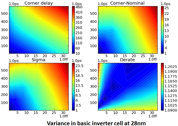 The upper left plot shows delay as a function of load and slew at the slow
corner (SS). The narrow bar shows the scale of actual delays in psec, where
the delay can range from 10 psec all the way up to 460 psec depending on
output load and input slew.
The plot on the bottom left shows sigma ("s", the standard deviation) at the
same load slew points, which can range from 1 psec all the way to 23.5 psec;
which at 3 sigma could be 30% to 50% over base delay.
The plots on the right convert the sigma and base delay information into
potential derates.
These first order influences also impact margins:
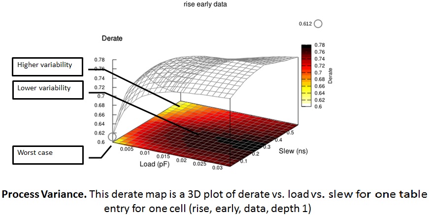
- Process Variance -- Too many corners.
Process variance is the root problem. It has always been there
but the foundry was able to manage it with enough margin for
designers to be competitive. The social contract was that the
foundries, over a few years, squeeze the process and deliver
acceptable yields. This has become increasingly not the case.
The spread between device corners (SS, FF) is worse than ever,
and the back end-of-line issues surrounding metal, vias, power,
and routing are just as bad.
The result is an explosion of the number of corners that must be
evaluated during physical design and timing -- literally 100's of
incremental corners. The spread between corners gets even worse
at low voltages. Other effects, like slew degradation, clock
skew/uncertainty, or device process variance, are all magnified at
these small geometries.
- Design Scale -- Millions of potential paths
There are literally millions of potential static paths on a quad
core phone chip, and growing. 10's of 1,000's of these paths
will be at or near failing at any given corner. The impact of
reducing power on the chip brings even "safe" timing paths right
up to the edge of failing.
- Complex Electrical Architectures -- Performance/Power/Voltage
To achieve aggressive power specifications such as 5 watts, yet
still be able to deliver near instantaneous high performance,
mobile and wireless chip teams have had to adopt some very complex
electrical architectures, particularly around voltage.
Using different voltage domains for digital and analog functions
is no longer sufficient. At 20 nm and below requires both
overdriving the design for performance and low voltage operation
to save power -- as low as 0.6 volts. This adds more corners, and,
when a transistor is operated at 0.6 volts or has a very slow ramp,
variance is exaggerated.
And for every Process-Voltage-Temperature (PVT) corner at the device level,
yet another library is required.
RULE-OF-THUMB MARGINING IS BROKEN
Most existing approaches still use rules-of-thumb to manage design margin
and process variance. Further, they depend on the foundry achieving high
yields in time for volume production.
The way traditional rule-of-thumb margins works is that:
1. The foundry would give their customer's foundry interface team
a chip variation margin number like 10% -- or today 20%.
2. This information went straight to the chip physical design team
and maybe a sign-off guru somewhere, who would then agree how to
apply the number.
3. The chip physical design team would then apply rule-of-thumb
margin to make everything work. They would set the clock speed
to 20% higher to push the data side to go fast, and then apply
the OCV number, and then some to the clock side to protect
against hold violations -- which are clock speed independent.
At 20 nm and below, this is no longer realistic. Rule-of-thumb margining is
over -- there is no longer enough margin. Gross percentage adjustments for
On Chip Variation (OCV) from the foundry can run as high as 20%, and when
combined with padding for clocks, jitter, voltage, and local temperature, it
becomes impossible to close timing at all corners at target power and speed.
Below is a common scenario - and it does flow downhill.
1. The chip physical design team yells at the library team, saying
their derate numbers are ridiculously pessimistic.
2. The library team yells at the foundry interface team that the
foundry' OCV number of 20% is unusable.
3. The silicon methodology team reminds everyone about the hold
violation they once had on a chip -- and that adding extra
margin is the only way to safely proceed.
4. The foundry itself is pretty much silent since they are focused
on trying to get the miracle of 16 nm and 14 nm into basic
readiness -- and rely on the ecosystem for solutions.
Loop back to Step 1 and repeat infinitely.
HOGAN'S 50/80 RULE OF 1ST ORDER TOOL EMERGENCE
After too many years of observation I've discovered a new EDA tech rule:
"When something starts go over 50% in impact,
80% of the time, you will need to break it
down with a better solution."
Some historical examples:
- When wire delay got to be over 50% of total delay 80% of the time,
we added parasitic extraction to get better numbers for wires.
- When crosstalk noise began to become more than 50% of cell delay,
we added Signal Integrity.
- When 2D parasitic error crossed over 50%, we added 2.5D, which we
recently had to improve again.
The same is true with IR drop, variance in custom, etc.
The upper left plot shows delay as a function of load and slew at the slow
corner (SS). The narrow bar shows the scale of actual delays in psec, where
the delay can range from 10 psec all the way up to 460 psec depending on
output load and input slew.
The plot on the bottom left shows sigma ("s", the standard deviation) at the
same load slew points, which can range from 1 psec all the way to 23.5 psec;
which at 3 sigma could be 30% to 50% over base delay.
The plots on the right convert the sigma and base delay information into
potential derates.
These first order influences also impact margins:
- Process Variance -- Too many corners.
Process variance is the root problem. It has always been there
but the foundry was able to manage it with enough margin for
designers to be competitive. The social contract was that the
foundries, over a few years, squeeze the process and deliver
acceptable yields. This has become increasingly not the case.
The spread between device corners (SS, FF) is worse than ever,
and the back end-of-line issues surrounding metal, vias, power,
and routing are just as bad.
The result is an explosion of the number of corners that must be
evaluated during physical design and timing -- literally 100's of
incremental corners. The spread between corners gets even worse
at low voltages. Other effects, like slew degradation, clock
skew/uncertainty, or device process variance, are all magnified at
these small geometries.
- Design Scale -- Millions of potential paths
There are literally millions of potential static paths on a quad
core phone chip, and growing. 10's of 1,000's of these paths
will be at or near failing at any given corner. The impact of
reducing power on the chip brings even "safe" timing paths right
up to the edge of failing.
- Complex Electrical Architectures -- Performance/Power/Voltage
To achieve aggressive power specifications such as 5 watts, yet
still be able to deliver near instantaneous high performance,
mobile and wireless chip teams have had to adopt some very complex
electrical architectures, particularly around voltage.
Using different voltage domains for digital and analog functions
is no longer sufficient. At 20 nm and below requires both
overdriving the design for performance and low voltage operation
to save power -- as low as 0.6 volts. This adds more corners, and,
when a transistor is operated at 0.6 volts or has a very slow ramp,
variance is exaggerated.
And for every Process-Voltage-Temperature (PVT) corner at the device level,
yet another library is required.
RULE-OF-THUMB MARGINING IS BROKEN
Most existing approaches still use rules-of-thumb to manage design margin
and process variance. Further, they depend on the foundry achieving high
yields in time for volume production.
The way traditional rule-of-thumb margins works is that:
1. The foundry would give their customer's foundry interface team
a chip variation margin number like 10% -- or today 20%.
2. This information went straight to the chip physical design team
and maybe a sign-off guru somewhere, who would then agree how to
apply the number.
3. The chip physical design team would then apply rule-of-thumb
margin to make everything work. They would set the clock speed
to 20% higher to push the data side to go fast, and then apply
the OCV number, and then some to the clock side to protect
against hold violations -- which are clock speed independent.
At 20 nm and below, this is no longer realistic. Rule-of-thumb margining is
over -- there is no longer enough margin. Gross percentage adjustments for
On Chip Variation (OCV) from the foundry can run as high as 20%, and when
combined with padding for clocks, jitter, voltage, and local temperature, it
becomes impossible to close timing at all corners at target power and speed.
Below is a common scenario - and it does flow downhill.
1. The chip physical design team yells at the library team, saying
their derate numbers are ridiculously pessimistic.
2. The library team yells at the foundry interface team that the
foundry' OCV number of 20% is unusable.
3. The silicon methodology team reminds everyone about the hold
violation they once had on a chip -- and that adding extra
margin is the only way to safely proceed.
4. The foundry itself is pretty much silent since they are focused
on trying to get the miracle of 16 nm and 14 nm into basic
readiness -- and rely on the ecosystem for solutions.
Loop back to Step 1 and repeat infinitely.
HOGAN'S 50/80 RULE OF 1ST ORDER TOOL EMERGENCE
After too many years of observation I've discovered a new EDA tech rule:
"When something starts go over 50% in impact,
80% of the time, you will need to break it
down with a better solution."
Some historical examples:
- When wire delay got to be over 50% of total delay 80% of the time,
we added parasitic extraction to get better numbers for wires.
- When crosstalk noise began to become more than 50% of cell delay,
we added Signal Integrity.
- When 2D parasitic error crossed over 50%, we added 2.5D, which we
recently had to improve again.
The same is true with IR drop, variance in custom, etc.
 And now that process variance has gotten over 50% of cell delay, shifting to
3D AOCV plus using systematic margining techniques is inevitable.
---- ---- ---- ---- ---- ---- ----
20 AND 14 NM DESIGNS REQUIRE "SYSTEMATIC MARGINING"
We must be able to add guard bands when needed, yet be able to reduce them
safely to create predictable timing margins for power optimization, and
yield at speed.
- Reduce guard bands too much, and you may miss your clock speeds,
or worse yet, get a hold violation that kills yield completely.
- Leave the guard bands too high, and you consumes unnecessary
power, and slows down your design.
A more disciplined "Systematic Margining" process is the only way to reach
target yields for performance and power at 20 and 14 nm, while avoiding
these problems.
Systematic Margining reduces guard bands by replacing rule-of-thumb
approaches with SPICE-accurate metrics to deliver a much more accurate
margin analysis in libraries, which propagate to SoC level. Data,
analytics, and tools are added to give a more accurate and complete picture
of the actual performance and yield characteristics of a library, IP or a
full SoC design.
Specifically, the cell design and characterization teams must create base
margining data that more accurately reflects variation at 20 nm and 14 nm.
The library team lays out the cells and the characterization team runs
SPICE to generation timing models and derates.
This new margin data ties back to circuit level data. The chip physical
design teams input the base margining data in -- setting their margins,
uncertainty values and corners to safely -- but not excessively, to cover
the potential variance.
And now that process variance has gotten over 50% of cell delay, shifting to
3D AOCV plus using systematic margining techniques is inevitable.
---- ---- ---- ---- ---- ---- ----
20 AND 14 NM DESIGNS REQUIRE "SYSTEMATIC MARGINING"
We must be able to add guard bands when needed, yet be able to reduce them
safely to create predictable timing margins for power optimization, and
yield at speed.
- Reduce guard bands too much, and you may miss your clock speeds,
or worse yet, get a hold violation that kills yield completely.
- Leave the guard bands too high, and you consumes unnecessary
power, and slows down your design.
A more disciplined "Systematic Margining" process is the only way to reach
target yields for performance and power at 20 and 14 nm, while avoiding
these problems.
Systematic Margining reduces guard bands by replacing rule-of-thumb
approaches with SPICE-accurate metrics to deliver a much more accurate
margin analysis in libraries, which propagate to SoC level. Data,
analytics, and tools are added to give a more accurate and complete picture
of the actual performance and yield characteristics of a library, IP or a
full SoC design.
Specifically, the cell design and characterization teams must create base
margining data that more accurately reflects variation at 20 nm and 14 nm.
The library team lays out the cells and the characterization team runs
SPICE to generation timing models and derates.
This new margin data ties back to circuit level data. The chip physical
design teams input the base margining data in -- setting their margins,
uncertainty values and corners to safely -- but not excessively, to cover
the potential variance.
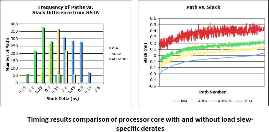 The chart above analyzes a processor core with and without derates. The
best outcome is illustrated by full statistical analysis. PBA with OCV
delivers the most pessimistic result. Applying AOCV and a 3D AOCV (complete
load slew derates) materially improves the slack in the overall design.
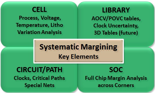
SYSTEMATIC MARGINING OF KEY ELEMENTS
Margin is a product of characterization. To examine margin, first you must
characterize at each level of abstraction. With Systematic Margining,
margins must be set accurately at ALL design levels, as shown below:
The chart above analyzes a processor core with and without derates. The
best outcome is illustrated by full statistical analysis. PBA with OCV
delivers the most pessimistic result. Applying AOCV and a 3D AOCV (complete
load slew derates) materially improves the slack in the overall design.
SYSTEMATIC MARGINING OF KEY ELEMENTS
Margin is a product of characterization. To examine margin, first you must
characterize at each level of abstraction. With Systematic Margining,
margins must be set accurately at ALL design levels, as shown below:
 This new data flows impacts many members of the development teams. As
things have been getting harder, the sign-off guru described earlier has
been morphing into the silicon methodology team. The library team must now
get involved to hand to pick up responsibility for derates. The chip
physical design team is now much more of a consumer of margin data than
magicians. Virtually the entire team, including cell designers and
characterization teams all have some role.
The Cell Level:
With systematic margins, cells are characterized past the basic noise and
delay models, with critical data added which can be considered in the
physical design and sign-off flows.
1. Each cell is individually characterized for process variance
across all load slew points, arcs, and PVT corners. This can be
used to select or eliminate cells, compare libraries across
foundries, and generate process derate tables for use in
sign-off timing flows. To generate good derates for 20 and 14
nm, teams must literally generate a complete set of variance
data for every possible load/slew/arc combination through a
cell. This must be repeated at every process voltage and
temperature corner. The new chips no longer just run at 2
voltages with voltage guardbands. They may now run at 4 or 5
voltage points (0.6, 0.8, 1.0, 1.1, and 1.3).
2. Clock cells are characterized for local temperature and voltage
sensitivity. The "flat" derates can be combined with process
derates to provide additional margining.
3. Flops and latches are characterized for timing constraints with
process variance. These elements can be combined into the basic
timing constraints used in the library, or factored into the
static timing clock skew or uncertainty settings.
The Library Level:
Basic derate tables and factors must be created that will be used by static
timing analysis and physical design tools. To do this there is more
behavior that is required for AOVC and POVC tables.
1. Library teams assemble derate tables such as AOCV and POCV to
model process, voltage and temperature at the SoC level.
- AOCV tables model manufacturing variation. The tables include
separate derate factors for each cell based on the depth of
the logic, or stages, for both clock and data paths. This
depth helps to take into account local on-die variation
independently from global die to die variation.
- Today's stage-based AOCV tables work with all of the major
static timing and optimization tools, and can be adopted with
no changes to the primary tool flow. AOCV and can be applied
by traditional timing and optimization tools without requiring
full statistical timing analysis.
- POCV is an alternative way to express variance that was
developed by Extreme DA, and is now being discussed by
Synopsys. POCV represents variance as a sigma -- lower case
sigma (s) which, in statistics, is the symbol used for
standard deviation, and s2 is known as the variance -- that
gets applied using statistical addition to adjust delay. It
models the same effects as AOCV, but applies the adjustment
to a global corner (SSG or FFG) instead of the traditional
timing corners (SS or FF).
- Note that the current generations of AOCV and POCV have
limitations. Because POCV as originally implemented only
allows 2 coefficients per cell, and AOCV only allows for 4
clock and 4 data values per cell -- even a simple inverter
could have 200 potential derates or 100 potential sigmas; you
have to mine all this data to find safe and sane derates.
2. SoC physical design teams assess the impact of these tables on
the timing of their design, and to redesign the table as
appropriate to fit their design rules (load/slew ranges, depth
factors, etc.)
3. Sign-off methodology teams set constraint clock uncertainty
factors to account for skew, jitter, process variation, etc.
When properly consumed by the optimization teams, these library-level derate
tables also help to insure that any optimizations for power or delay do not
unintentionally inject variance.
The Circuit/Path Level:
There are a number of cases where chip teams want to analyze special nets at
SPICE accuracy. They can cross blocks, or even the large parts of the chip.
Designers may simply validate the paths for accuracy, or they may feed
corrected timing back into the STA tool. A couple of examples of special
paths are clocks and busses.
1. Circuit accurate analysis of clock trees enables designers to
replace estimated delay with actual delay values.
2. SPICE-accurate path analysis can be applied to accurate assess
which paths are truly failing, and which can be waived. When
combined with actual voltage or temperature variation, this can
give a better assessment of the actual total margin in the chip.
Keep in mind that circuit level accuracy is only used wherever appropriate.
Doing it eveywhere for all paths is too time/CPU/engineering consuming.
The Full Chip Level:
Finally, the full chip needs to be evaluated from the standpoint of margin.
1. Full chip timing reports with variance analysis across corners.
When possible, variance impact can be adjusted post timing to
assess actual timing and power margin across PVT corners. These
analyses can be applied on graph or path based timing.
2. Late stage power and timing optimization with variance. Any
late stage ECO or optimization flows have to take margin into
account.
Each of these margin applications injects silicon realism into the physical
design and sign-off flows. Power optimizations that might have seemed
attractive -- reducing the drive strength or VT of a cell in a path-- may be
rejected or limited because of the variance risk.
Equally important, much of the guess work in setting margins is eliminated.
The overall attraction to this approach is that the sign-off for power and
timing is a much better predictor of silicon performance.
The final result? Variance tolerant, high yield designs.
---- ---- ---- ---- ---- ---- ----
SYSTEMATIC MARGINING KEY PLAYERS
Here's my current snapshot of the 3 known players that do margining:
1. Cadence. Cadence offers Virtuoso Liberate. Liberate provides
both general lib characterization, and basic derate calculation.
Cadence PD and STA tools support AOCV and MCMM. Their timing
and power optimization tools also support AOCV with sign-off
accurate validation using path-based analysis.
2. CLK-DA. CLK-DA offers tools which support Systematic
Margining at the cell, library, path and SoC level: AOCV FX,
Path FX and Margin FX. AOCV FX generates both AOCV and POCV
derate tables as well as constraint uncertainty that can be used
by all of the major PD tools, and can support the proposed full
load/slew/arc tables as well. AOCV FX has been extended to
support library level voltage and process sensitivity as well.
Path FX is a high accuracy path based timing analyzer that can
be applied to critical paths, clocks or other important SoC
signals. Margin FX is a set of utilities for analyzing margin
at the full chip level, including evaluating the impact of
alternative derates.
3. Synopsys. Like Cadence, Synopsys offers a basic derate tool for
characterization with its (Magma) SiliconSmart. Its timing and
physical design tools support AOCV, and their late stage
power reduction and optimization tools also use AOCV.
They have also continued to support POCV from Extreme DA and
have added it to the mix of derate tools for future extension
of Liberty and other margining flows.
There is an intense level of activity surrounding systematic margining at
the standards level as well. The Liberty Technology Advisory Board (TAB) is
considering adding AOCV and POCV-like capabilities to the library, and
addressing their current limitations by adding full load/slew/arc specific
data to the derates and coefficients. Systematic Margining will rely on
these new formats and other innovations to continue bring the realities of
20 and 14 nm silicon into the SoC design flow.
Once again, I invite others to share their thoughts on this discussion.
- Jim Hogan
Vista Ventures, LLC Los Gatos, CA
Editor's Note: Jim Hogan is on the CLK-DA board of Directors. - John
This new data flows impacts many members of the development teams. As
things have been getting harder, the sign-off guru described earlier has
been morphing into the silicon methodology team. The library team must now
get involved to hand to pick up responsibility for derates. The chip
physical design team is now much more of a consumer of margin data than
magicians. Virtually the entire team, including cell designers and
characterization teams all have some role.
The Cell Level:
With systematic margins, cells are characterized past the basic noise and
delay models, with critical data added which can be considered in the
physical design and sign-off flows.
1. Each cell is individually characterized for process variance
across all load slew points, arcs, and PVT corners. This can be
used to select or eliminate cells, compare libraries across
foundries, and generate process derate tables for use in
sign-off timing flows. To generate good derates for 20 and 14
nm, teams must literally generate a complete set of variance
data for every possible load/slew/arc combination through a
cell. This must be repeated at every process voltage and
temperature corner. The new chips no longer just run at 2
voltages with voltage guardbands. They may now run at 4 or 5
voltage points (0.6, 0.8, 1.0, 1.1, and 1.3).
2. Clock cells are characterized for local temperature and voltage
sensitivity. The "flat" derates can be combined with process
derates to provide additional margining.
3. Flops and latches are characterized for timing constraints with
process variance. These elements can be combined into the basic
timing constraints used in the library, or factored into the
static timing clock skew or uncertainty settings.
The Library Level:
Basic derate tables and factors must be created that will be used by static
timing analysis and physical design tools. To do this there is more
behavior that is required for AOVC and POVC tables.
1. Library teams assemble derate tables such as AOCV and POCV to
model process, voltage and temperature at the SoC level.
- AOCV tables model manufacturing variation. The tables include
separate derate factors for each cell based on the depth of
the logic, or stages, for both clock and data paths. This
depth helps to take into account local on-die variation
independently from global die to die variation.
- Today's stage-based AOCV tables work with all of the major
static timing and optimization tools, and can be adopted with
no changes to the primary tool flow. AOCV and can be applied
by traditional timing and optimization tools without requiring
full statistical timing analysis.
- POCV is an alternative way to express variance that was
developed by Extreme DA, and is now being discussed by
Synopsys. POCV represents variance as a sigma -- lower case
sigma (s) which, in statistics, is the symbol used for
standard deviation, and s2 is known as the variance -- that
gets applied using statistical addition to adjust delay. It
models the same effects as AOCV, but applies the adjustment
to a global corner (SSG or FFG) instead of the traditional
timing corners (SS or FF).
- Note that the current generations of AOCV and POCV have
limitations. Because POCV as originally implemented only
allows 2 coefficients per cell, and AOCV only allows for 4
clock and 4 data values per cell -- even a simple inverter
could have 200 potential derates or 100 potential sigmas; you
have to mine all this data to find safe and sane derates.
2. SoC physical design teams assess the impact of these tables on
the timing of their design, and to redesign the table as
appropriate to fit their design rules (load/slew ranges, depth
factors, etc.)
3. Sign-off methodology teams set constraint clock uncertainty
factors to account for skew, jitter, process variation, etc.
When properly consumed by the optimization teams, these library-level derate
tables also help to insure that any optimizations for power or delay do not
unintentionally inject variance.
The Circuit/Path Level:
There are a number of cases where chip teams want to analyze special nets at
SPICE accuracy. They can cross blocks, or even the large parts of the chip.
Designers may simply validate the paths for accuracy, or they may feed
corrected timing back into the STA tool. A couple of examples of special
paths are clocks and busses.
1. Circuit accurate analysis of clock trees enables designers to
replace estimated delay with actual delay values.
2. SPICE-accurate path analysis can be applied to accurate assess
which paths are truly failing, and which can be waived. When
combined with actual voltage or temperature variation, this can
give a better assessment of the actual total margin in the chip.
Keep in mind that circuit level accuracy is only used wherever appropriate.
Doing it eveywhere for all paths is too time/CPU/engineering consuming.
The Full Chip Level:
Finally, the full chip needs to be evaluated from the standpoint of margin.
1. Full chip timing reports with variance analysis across corners.
When possible, variance impact can be adjusted post timing to
assess actual timing and power margin across PVT corners. These
analyses can be applied on graph or path based timing.
2. Late stage power and timing optimization with variance. Any
late stage ECO or optimization flows have to take margin into
account.
Each of these margin applications injects silicon realism into the physical
design and sign-off flows. Power optimizations that might have seemed
attractive -- reducing the drive strength or VT of a cell in a path-- may be
rejected or limited because of the variance risk.
Equally important, much of the guess work in setting margins is eliminated.
The overall attraction to this approach is that the sign-off for power and
timing is a much better predictor of silicon performance.
The final result? Variance tolerant, high yield designs.
---- ---- ---- ---- ---- ---- ----
SYSTEMATIC MARGINING KEY PLAYERS
Here's my current snapshot of the 3 known players that do margining:
1. Cadence. Cadence offers Virtuoso Liberate. Liberate provides
both general lib characterization, and basic derate calculation.
Cadence PD and STA tools support AOCV and MCMM. Their timing
and power optimization tools also support AOCV with sign-off
accurate validation using path-based analysis.
2. CLK-DA. CLK-DA offers tools which support Systematic
Margining at the cell, library, path and SoC level: AOCV FX,
Path FX and Margin FX. AOCV FX generates both AOCV and POCV
derate tables as well as constraint uncertainty that can be used
by all of the major PD tools, and can support the proposed full
load/slew/arc tables as well. AOCV FX has been extended to
support library level voltage and process sensitivity as well.
Path FX is a high accuracy path based timing analyzer that can
be applied to critical paths, clocks or other important SoC
signals. Margin FX is a set of utilities for analyzing margin
at the full chip level, including evaluating the impact of
alternative derates.
3. Synopsys. Like Cadence, Synopsys offers a basic derate tool for
characterization with its (Magma) SiliconSmart. Its timing and
physical design tools support AOCV, and their late stage
power reduction and optimization tools also use AOCV.
They have also continued to support POCV from Extreme DA and
have added it to the mix of derate tools for future extension
of Liberty and other margining flows.
There is an intense level of activity surrounding systematic margining at
the standards level as well. The Liberty Technology Advisory Board (TAB) is
considering adding AOCV and POCV-like capabilities to the library, and
addressing their current limitations by adding full load/slew/arc specific
data to the derates and coefficients. Systematic Margining will rely on
these new formats and other innovations to continue bring the realities of
20 and 14 nm silicon into the SoC design flow.
Once again, I invite others to share their thoughts on this discussion.
- Jim Hogan
Vista Ventures, LLC Los Gatos, CA
Editor's Note: Jim Hogan is on the CLK-DA board of Directors. - John
Join
Index
Next->Item
|
|


