( ESNUG 534 Item 6 ) -------------------------------------------- [11/15/13]
From: [Trent McConaghy of Solido Design]
Subject: Solido brainiac Trent on CICC'13 analog, memory, FinFET, variation
Hi John,
The Custom Integrated Circuits Conference (CICC) 2013 took place on Monday,
Sept 23rd through Wednesday, Sept 25th at the Doubletree Hotel in San Jose,
California.
About 300 custom circuit designers and custom CAD engineers attended CICC.
The conference had 5 simultaneous threads of technical papers, panels, and
education sessions. Mark Horowitz of Stanford gave the keynoted on formal
composition of analog circuits (his work is at ESNUG 518 #6.)
Below, I report on some of the papers at CICC 2013 that caught my interest
on topics of variation, reliability, analog/mixed-signal CAD, memory CAD,
and more.
- Trent McConaghy, CTO
Solido Design Automation Saskatoon, Canada
---- ---- ---- ---- ---- ---- ----
PROCESS VARIATION + ANALOG
Paper: Corner Models: Inaccurate at Best, and it Only Gets Worst
Authors: Colin McAndrew et al (Freescale)
This paper describes how digital CMOS corner models have major inaccuracies
for analyzing variation of analog circuits, and shows how related "standard"
design practices are dangerous. Colin, his colleagues, and many others in
academia and industry have known about this problem for a long time, and
have spent considerable effort developing solutions. Interestingly, there
was never a publication that examined the issue in detail; this paper
changes that.
A change in a circuit performance measure is a function of the sensitivity
of that measure to each process variable, and the change in each process
variable compared to nominal. The fundamental issue is that corner models
assume a fixed change in process variables, ignorant of the sensitivities.
Therefore, the models "guarantee nothing about what the sigma-level
variation in [performance] will be".
To illustrate the issue, Figure 1 below compares the gold standard for
accuracy (Monte Carlo total = Monte Carlo local + Monte Carlo global, in
blue) compared to different corner models (MOS, C, MOS/C/R) and variation
models (Monte Carlo just global), for a 2-stage 48-transistor opamp on 90 nm
CMOS, on four different performance measures.
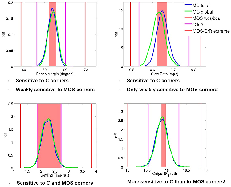 Fig 1: Comparison of Monte Carlo total, versus less accurate
approaches, on four 90 nm opamp outputs. Ref: McAndrew
et al, CICC 2013. (click pic to enlarge)
A common practice is to simulate local variation top of global digital
process corners. However, this is inaccurate for two reasons:
(a) it implicitly assumes that the standard deviations of global
variation and local variations add, when the correct
mathematical treatment is to add the variances
(b) as discussed above, variations (global or otherwise) cannot be
independent of the performance sensitivities
Fig 2 illustrates the problem, comparing the gold standard for accuracy
(global + local) to just global, and to worst-case/best-case + local.
Fig 1: Comparison of Monte Carlo total, versus less accurate
approaches, on four 90 nm opamp outputs. Ref: McAndrew
et al, CICC 2013. (click pic to enlarge)
A common practice is to simulate local variation top of global digital
process corners. However, this is inaccurate for two reasons:
(a) it implicitly assumes that the standard deviations of global
variation and local variations add, when the correct
mathematical treatment is to add the variances
(b) as discussed above, variations (global or otherwise) cannot be
independent of the performance sensitivities
Fig 2 illustrates the problem, comparing the gold standard for accuracy
(global + local) to just global, and to worst-case/best-case + local.
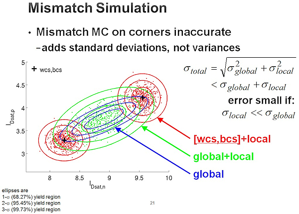 Fig 2: Adding standard deviations, rather than variances, induces
errors. The plot compares Monte Carlo total (global + local),
versus less accurate approaches. Ref: McAndrew, CICC 2013
(click pic to enlarge)
Finally, McAndrew et al described how, even in the lucky case if a digital
corner is accurate on one dimension, they become increasingly pessimistic
as the number of process parameters n increases. The implied target yield
is 3-sigma total, but digital corners go out a distance of 3-sigma for each
dimension, or (3*SQRT(n))-sigma total. This leads to overdesign by a factor
of SQRT(n) -- needlessly compromising power, performance, and area. Fig 3
illustrates. Consider a typical 50-device circuit with 10 local process
variables per device, and 10 global process variables, or n= 50*10+10 = 510.
Designing it with 3-sigma digital corners over-designs the circuit by a
factor of SQRT(510) = 22.6x.
Fig 2: Adding standard deviations, rather than variances, induces
errors. The plot compares Monte Carlo total (global + local),
versus less accurate approaches. Ref: McAndrew, CICC 2013
(click pic to enlarge)
Finally, McAndrew et al described how, even in the lucky case if a digital
corner is accurate on one dimension, they become increasingly pessimistic
as the number of process parameters n increases. The implied target yield
is 3-sigma total, but digital corners go out a distance of 3-sigma for each
dimension, or (3*SQRT(n))-sigma total. This leads to overdesign by a factor
of SQRT(n) -- needlessly compromising power, performance, and area. Fig 3
illustrates. Consider a typical 50-device circuit with 10 local process
variables per device, and 10 global process variables, or n= 50*10+10 = 510.
Designing it with 3-sigma digital corners over-designs the circuit by a
factor of SQRT(510) = 22.6x.
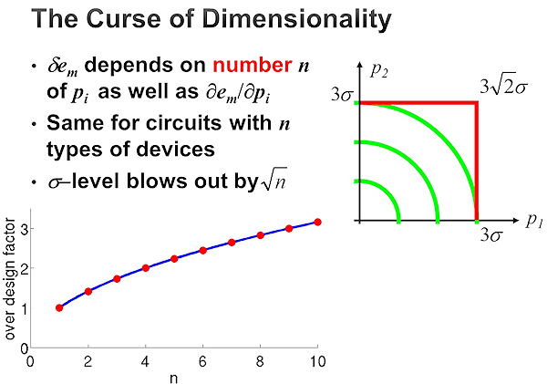 Fig 3: Designing with digital MOS corners causes overdesign by a
factor of SQRT(n). Ref: McAndrew, CICC'13 (click to enlarge)
To address these issues, McAndrew et al recommend that "corner models should
be generated on a circuit performance-by-performance basis, and can change
as device geometries and biases change even for one circuit topology," and
"Do not request physically unrealistic corners. Do use Monte Carlo".
---- ---- ---- ---- ---- ---- ----
Paper: Indirect Performance Sensing for On-Chip Analog Self-Healing
via Bayesian Model Fusion
Authors: Shupeng Sun et al (Carnegie Mellon, plus IBM, Oregon State)
The overall aim is to improve yield of analog circuits, post-manufacturing,
via "self-healing" circuits. This paper tested the approach on a Colpitts
VCO on a 32nm CMOS SOI process, for the output phase noise at 25GHz. Since
phase noise at such a high frequency is hard to measure, the idea is to tune
each chip with feedback from an *estimate* of phase noise. The estimate is
based on a quadratic model of four easier-to-measure outputs: oscillation
frequency, oscillation amplitude, bias current, and bias voltage.
To demonstrate the methodology, the authors performed the following steps
from a first and second wafer:
1) From the first wafer, do off-chip tests for all VCOs, and
estimate the initial model parameters
2) From the second wafer, do off-chip tests for just a few VCOs.
3) Recalibrate the initial model parameters using "Bayesian Model
Fusion" (BMF) on the second wafer's data. BMF applies Bayes'
method to reconcile the new measurement data with the previous
parameter estimates.
4) "Self-heal" every VCO on the second wafer. Here, self-healing
simply tests each possible bias voltages (set by the DAC), and
remembers the one with the minimum estimated phase noise.
The authors found that, using this BMF approach, the yield of the second
wafer could be raised from 0% to 69.2% by measuring just a single VCO.
Previous approaches would take four measured VCOs to get similar yield.
If all 61 VCOs were measured (the ideal, but expensive), the yield would
be 78.7%.
---- ---- ---- ---- ---- ---- ----
Paper: Structure-Aware High-Dimensional Performance Modeling for
Analog and Mixed-Signal Circuits
Authors: Shupeng Sun and Xin Li (Carnegie Mellon) and Chenjie Gu (Intel)
The problem space is creating models that map thousands of process variables
to an output performance value. The training data comes from SPICE
simulations. The challenge is to maximize model accuracy and minimize the
number of training samples (simulations). The state of the art in building
such models uses recently-developed linear regression techniques, such as
orthogonal matching pursuit (OMP) or elastic nets.
This paper showed a new approach to improve the accuracy vs. simulations
tradeoff, by using a priori knowledge to group process parameters. Example
groups are:
- all the delta_VT's for each multiplier in a transistor
- all the delta_VT's for each transistor in a differential pair.
The algorithm proceeds in an iterative loop until convergence, exploiting
the grouping knowledge. At each iteration, the algorithm identifies the
next important group, and then finds nonzero model parameters for the
variables in that group.
For the same accuracy compared to the previous OMP approach, this technique
needed 2.5x fewer simulations.
---- ---- ---- ---- ---- ---- ----
Paper: Discretization and Discrimination Methods for Design,
Verification, and Testing of Analog/Mixed-Signal Circuits
Authors: Jaeha Kim et al (Seoul National University)
The core idea in the work is that one may take advantage of under process
variation to *simplify* algorithmic challenges in analog CAD. Specifically,
in analogy to an information-theory additive noise channel model, one can
use process variation to choose a minimum spacing, discretizing the search
space of interest (e.g. the sizing space).
The authors illustrated this approach in three separate problem domains:
- analog circuit sizing,
- verifying a circuit's correct convergence to the operating mode
- quantifying a test's fault coverage.
The authors showed how measuring correlation among the circuit responses
(e.g. bandwidth) can be used to improve the approach.
---- ---- ---- ---- ---- ---- ----
PROCESS VARIATION + MEMORY
Paper: SRAM Read Current Variability and its dependence on
Transistor Statistics
Authors: Sriram Venugopalan (UC Berkeley) et al (GlobalFoundries)
The authors investigated a new technique to efficiently estimate read
current (Iread) distribution of SRAM bitcells.
Working from first principles, the technique reduces Iread variability down
to simply a function of individual transistor variability. Specifically,
Iread variability is a function of
(a) gate overdrive voltage variation of the pass-gate (PG) and
pull-down (PD) devices;
(b) local threshold voltage variation, and
(c) cell ratio, i.e. the ratio of PD saturation current to PG
saturation current. The authors introduce the "stack
variability" concept to relate PG/PD variability to a single
device.
Leveraging these concepts, the authors could efficiently estimate Iread at
6-sigma using the voltage acceleration method (VAM). Given that the
approach is for SRAM readability (but not writeability), this technique will
be particularly useful where writeability is not a constraint, such as
8T-SRAM cells.
---- ---- ---- ---- ---- ---- ----
MOORE'S LAW + FINFETS
Paper: From 2D-Planar to 3D-Non-Planar Device Architecture,
A Scalable Path Forward
Author: Ghavam Shahidi (IBM)
The paper investigated the benefits and challenges of moving from planar
CMOS to FinFETs.
First, it reviewed the benefits of Moore's Law: each node has reduced x-
and y- dimensions by 30%, area reduction of 50%, and 30% drop in power (due
to drop in transistor width, and therefore capacitance). The Dennard
scaling performance numbers, as measured by ring oscillator frequency, point
to a 17% / year improvement between 1995 and 2010, and 10% since 2010. On
Intel and IBM microprocessor data, recent nodes have brought 33-50% power
reduction.
The paper then described how today's FinFETs differ to the ideal, in two
ways.
1) An ideal FinFET has no channel doping (i.e. fully depleted), and
therefore has no random dopant fluctuations (RDFs, a key
contributor of process variation), which allows for low voltage
operation. However, this only occurs at a low threshold voltage
(VT). Multiple VTs are needed to optimize a chip's logic-power
tradeoff: the lowest-VT is used for critical paths, the
highest-VT is used in SRAMs to minimize standby leakage, and
midrange VTs are used elsewhere.
To achieve multiple VTs, today's FinFETs actually introduce
doping, and therefore still have RDF variation, impacting SRAMs
and other circuitry. To summarize: in theory, FinFET SRAMs have
no RDF variability; in practice, they do.
2) An ideal FinFET has a thin body, to allow scaling to short
lengths, for low power operation and to easily fit into the
shrinking device pitch. However, today's FinFETs are tapered to
overcome manufacturing challenges. Unfortunately, it appears
that tapering will affect length for nodes below 14nm, getting in
the way of proper scaling.
To handle these two issues, researchers are exploring many options, both
with FinFETs and with planar CMOS devices.
---- ---- ---- ---- ---- ---- ----
AGING / RELIABILITY
Paper: Circuit Reliability Simulation Using TMI2
Authors: Min-Chie Jeng et al (TSMC)
Aging / reliability is degradation in circuit performance over time, due to
hot-carrier injection (HCI), bias-temperature instability (BTI), and more.
TMI is the TSMC Model Interface, which has become an industry standard model
interface for circuit simulators. Commercial simulators that comply with
TMI specifications "automatically have the TMI aging simulation capability".
Inside a TMI library are aging models, which sits beside the SPICE models
(e.g. BSIM). An aging model describes the degradation of device-level
performance characteristics (e.g. Idsat, VT) as a function of voltages,
current, temperatures, and time. TMI supports proprietary aging models
(via compilation), yet allows all simulators to use the same aging model
parameters. Aging simulation is simply running the simulator at different
values for time, using the degraded performance characteristics.
To create an aging model, engineers measure devices under different bias
conditions and temperatures to set values for the model's calibration
parameters. Due to the huge data gathering effort required, most aging
models have limitations:
- Poor support for the "degradation variation effect", i.e. aging
and statistical variation interact. This happens, for example,
even if a current mirror is perfectly matched at fabrication, its
devices may age at different rates, for so-called "mismatch
drift".
- Poor support for analog parameters like transconductance (gm) and
channel conductance (gds).
- Poor support for BTI recovery effect. The TMI models have a
partial workaround, via a user-set recovery value between 0%
recovery (pessimistic) and 100% recovery (optimistic).
- With these two limitations, it's inappropriate to simulate Vccmin
drift on SRAM cells, or aging on most analog circuits.
- Note that there *is* research that handles these limitations,
such as: E. Maricau and G. Gielen, Analog IC Reliability in
Nanometer CMOS, Springer, 2013.
The TSMC authors provide some useful guidelines to designers regarding aging
simulation:
- Accuracy is not at the accuracy level of SPICE models (yet).
Therefore, it's better to use relative aging numbers, rather than
absolutes.
- Aging models tend to err on the side of conservatism. Therefore
device lifetime may be better than what the aging models predict.
- Don't ask aging simulation to simulate where SPICE models are
inaccurate. For example, given that SPICE models are typically
characterized up to 1.2*Vdd, and from -40 degrees C to +125 C,
don't run aging model simulation at more extreme Vdds or
temperatures.
The TSMC authors described an alternative to full-fledged aging simulation:
the "End-of-Life" (EOL) model approach. EOL models can be thought of as
corners for aging, where all devices hit some end-of-life condition, such as
Idsat degradation hits 10%. For example, the counterparts to (fresh, age=0)
TT, FF, and SS models are EOL_TT, EOL_FF, and EOL_SS respectively. Then,
PVT analysis becomes PVTT analysis, where the last "T" is time.
The authors provide guidelines on EOL model usage:
1) Since EOL models are not fully realistic, it's better to assess
relative effects.
2) Apply EOL models only on devices under similar stresses.
As an example, EOL models are fine for SRAM pull-up devices. But for
digital logic, it should be on critical devices only, which are stressed the
most.
---- ---- ---- ---- ---- ---- ----
THERMAL NOISE MODELING
Paper: Thermal Noise Modeling of Nano-scale MOSFETs for Mixed-signal
and RF Applications
Authors: Chih-Hung Chen (UMC), David Chen (McMaster University) et al
As the paper states, "thermal noise is the undesired random fluctuation from
the electronic devices in circuits and added onto a signal." Thermal noise
bounds the performance not only for high-frequency circuits like low-noise
amplifiers (LNAs), but also for circuits like opamps when those circuits
have overcome the next-most dominant noise source (1/f noise). These bounds
ultimately affect user-level performance measures like battery life and
communication distance between wireless devices.
The paper describes the process of measuring thermal noise, then creating
models from those measurements. Interestingly (and perhaps unsurprisingly),
due to extreme frequencies and related challenges, measurements have high
uncertainty. In the example given, the channel thermal noise measurements
varied from -33% to +57%; the paper noted "significant spread in the
published noise factors."
The authors presented their physics-based approach to modeling thermal
noise, how it may be implemented in a simulator, and corner models. To
reduce the number of fitting parameters from two to a single process-
independent parameter, the authors leverage an atomistic TCAD device
simulator. The authors' thermal noise model works with a variety of compact
models, from BSIM4 (in the paper) to PSP, HiSIM, or EKV; and a variety of
simulators, from Spectre (in the paper) to HSPICE or Eldo.
The authors describe how engineering future device technologies should
consider channel thermal noise and device transconductance, through a
combined "noise sheet resistance" figure of merit.
---- ---- ---- ---- ---- ---- ----
MIXED-SIGNAL SIMULATION
Paper: Fast FPGA Emulation of Background-Calibrated SAR ADC with
Internal Redundancy Dithering
Authors: Guanhua Wang and Yun Chui (University of Texas)
The aim was to quickly simulate a SAR ADC (successive-approximation-register
analog-to-digital converter) with 14.5 bits and a digital background
calibration algorithm.
The traditional approach is to simulate the behavioral model on Matlab,
which takes 30 h. The authors instead compiled the behavioral model to
VHDL, ran an FPGA synthesis tool, put the synthesized code onto an Altera D4
FPGA board, and ran the FPGA. The runtime was 36 sec, or a 3000x speed-up.
---- ---- ---- ---- ---- ---- ----
NONLINEAR DISTORTION
Paper: A Model-Agnostic Technique for Simulating Per-Element
Distortion Contributions
Authors: Nagendra Krishnapura and Rakshitdatta K. S. of (IIT Madras)
The overall aim is to identify the relative impact of each device on
unwanted distortions due to nonlinearity and noise. Previous approaches
used Taylor (linear) or Volterra (quadratic) series descriptions of circuit
components, or other techniques.
This paper aims to make distortion analysis simple for a designer using a
conventional SPICE simulator. It approached the problem by showing how to
create a new nonlinear element that has the same operating point and linear
characteristics, but different nonlinear characteristics.
Designers use the approach by running multiple simulations of the total
output distortion of a circuit with slightly changed nonlinear
characteristics in the relevant element. The approach requires no knowledge
of the device model.
---- ---- ---- ---- ---- ---- ----
From my perspective, CICC 2013 had an excellent set of interesting papers
on analog variation and more. I hope your readers find my summary useful.
- Trent McConaghy, CTO
Solido Design Automation Saskatoon, Canada
Fig 3: Designing with digital MOS corners causes overdesign by a
factor of SQRT(n). Ref: McAndrew, CICC'13 (click to enlarge)
To address these issues, McAndrew et al recommend that "corner models should
be generated on a circuit performance-by-performance basis, and can change
as device geometries and biases change even for one circuit topology," and
"Do not request physically unrealistic corners. Do use Monte Carlo".
---- ---- ---- ---- ---- ---- ----
Paper: Indirect Performance Sensing for On-Chip Analog Self-Healing
via Bayesian Model Fusion
Authors: Shupeng Sun et al (Carnegie Mellon, plus IBM, Oregon State)
The overall aim is to improve yield of analog circuits, post-manufacturing,
via "self-healing" circuits. This paper tested the approach on a Colpitts
VCO on a 32nm CMOS SOI process, for the output phase noise at 25GHz. Since
phase noise at such a high frequency is hard to measure, the idea is to tune
each chip with feedback from an *estimate* of phase noise. The estimate is
based on a quadratic model of four easier-to-measure outputs: oscillation
frequency, oscillation amplitude, bias current, and bias voltage.
To demonstrate the methodology, the authors performed the following steps
from a first and second wafer:
1) From the first wafer, do off-chip tests for all VCOs, and
estimate the initial model parameters
2) From the second wafer, do off-chip tests for just a few VCOs.
3) Recalibrate the initial model parameters using "Bayesian Model
Fusion" (BMF) on the second wafer's data. BMF applies Bayes'
method to reconcile the new measurement data with the previous
parameter estimates.
4) "Self-heal" every VCO on the second wafer. Here, self-healing
simply tests each possible bias voltages (set by the DAC), and
remembers the one with the minimum estimated phase noise.
The authors found that, using this BMF approach, the yield of the second
wafer could be raised from 0% to 69.2% by measuring just a single VCO.
Previous approaches would take four measured VCOs to get similar yield.
If all 61 VCOs were measured (the ideal, but expensive), the yield would
be 78.7%.
---- ---- ---- ---- ---- ---- ----
Paper: Structure-Aware High-Dimensional Performance Modeling for
Analog and Mixed-Signal Circuits
Authors: Shupeng Sun and Xin Li (Carnegie Mellon) and Chenjie Gu (Intel)
The problem space is creating models that map thousands of process variables
to an output performance value. The training data comes from SPICE
simulations. The challenge is to maximize model accuracy and minimize the
number of training samples (simulations). The state of the art in building
such models uses recently-developed linear regression techniques, such as
orthogonal matching pursuit (OMP) or elastic nets.
This paper showed a new approach to improve the accuracy vs. simulations
tradeoff, by using a priori knowledge to group process parameters. Example
groups are:
- all the delta_VT's for each multiplier in a transistor
- all the delta_VT's for each transistor in a differential pair.
The algorithm proceeds in an iterative loop until convergence, exploiting
the grouping knowledge. At each iteration, the algorithm identifies the
next important group, and then finds nonzero model parameters for the
variables in that group.
For the same accuracy compared to the previous OMP approach, this technique
needed 2.5x fewer simulations.
---- ---- ---- ---- ---- ---- ----
Paper: Discretization and Discrimination Methods for Design,
Verification, and Testing of Analog/Mixed-Signal Circuits
Authors: Jaeha Kim et al (Seoul National University)
The core idea in the work is that one may take advantage of under process
variation to *simplify* algorithmic challenges in analog CAD. Specifically,
in analogy to an information-theory additive noise channel model, one can
use process variation to choose a minimum spacing, discretizing the search
space of interest (e.g. the sizing space).
The authors illustrated this approach in three separate problem domains:
- analog circuit sizing,
- verifying a circuit's correct convergence to the operating mode
- quantifying a test's fault coverage.
The authors showed how measuring correlation among the circuit responses
(e.g. bandwidth) can be used to improve the approach.
---- ---- ---- ---- ---- ---- ----
PROCESS VARIATION + MEMORY
Paper: SRAM Read Current Variability and its dependence on
Transistor Statistics
Authors: Sriram Venugopalan (UC Berkeley) et al (GlobalFoundries)
The authors investigated a new technique to efficiently estimate read
current (Iread) distribution of SRAM bitcells.
Working from first principles, the technique reduces Iread variability down
to simply a function of individual transistor variability. Specifically,
Iread variability is a function of
(a) gate overdrive voltage variation of the pass-gate (PG) and
pull-down (PD) devices;
(b) local threshold voltage variation, and
(c) cell ratio, i.e. the ratio of PD saturation current to PG
saturation current. The authors introduce the "stack
variability" concept to relate PG/PD variability to a single
device.
Leveraging these concepts, the authors could efficiently estimate Iread at
6-sigma using the voltage acceleration method (VAM). Given that the
approach is for SRAM readability (but not writeability), this technique will
be particularly useful where writeability is not a constraint, such as
8T-SRAM cells.
---- ---- ---- ---- ---- ---- ----
MOORE'S LAW + FINFETS
Paper: From 2D-Planar to 3D-Non-Planar Device Architecture,
A Scalable Path Forward
Author: Ghavam Shahidi (IBM)
The paper investigated the benefits and challenges of moving from planar
CMOS to FinFETs.
First, it reviewed the benefits of Moore's Law: each node has reduced x-
and y- dimensions by 30%, area reduction of 50%, and 30% drop in power (due
to drop in transistor width, and therefore capacitance). The Dennard
scaling performance numbers, as measured by ring oscillator frequency, point
to a 17% / year improvement between 1995 and 2010, and 10% since 2010. On
Intel and IBM microprocessor data, recent nodes have brought 33-50% power
reduction.
The paper then described how today's FinFETs differ to the ideal, in two
ways.
1) An ideal FinFET has no channel doping (i.e. fully depleted), and
therefore has no random dopant fluctuations (RDFs, a key
contributor of process variation), which allows for low voltage
operation. However, this only occurs at a low threshold voltage
(VT). Multiple VTs are needed to optimize a chip's logic-power
tradeoff: the lowest-VT is used for critical paths, the
highest-VT is used in SRAMs to minimize standby leakage, and
midrange VTs are used elsewhere.
To achieve multiple VTs, today's FinFETs actually introduce
doping, and therefore still have RDF variation, impacting SRAMs
and other circuitry. To summarize: in theory, FinFET SRAMs have
no RDF variability; in practice, they do.
2) An ideal FinFET has a thin body, to allow scaling to short
lengths, for low power operation and to easily fit into the
shrinking device pitch. However, today's FinFETs are tapered to
overcome manufacturing challenges. Unfortunately, it appears
that tapering will affect length for nodes below 14nm, getting in
the way of proper scaling.
To handle these two issues, researchers are exploring many options, both
with FinFETs and with planar CMOS devices.
---- ---- ---- ---- ---- ---- ----
AGING / RELIABILITY
Paper: Circuit Reliability Simulation Using TMI2
Authors: Min-Chie Jeng et al (TSMC)
Aging / reliability is degradation in circuit performance over time, due to
hot-carrier injection (HCI), bias-temperature instability (BTI), and more.
TMI is the TSMC Model Interface, which has become an industry standard model
interface for circuit simulators. Commercial simulators that comply with
TMI specifications "automatically have the TMI aging simulation capability".
Inside a TMI library are aging models, which sits beside the SPICE models
(e.g. BSIM). An aging model describes the degradation of device-level
performance characteristics (e.g. Idsat, VT) as a function of voltages,
current, temperatures, and time. TMI supports proprietary aging models
(via compilation), yet allows all simulators to use the same aging model
parameters. Aging simulation is simply running the simulator at different
values for time, using the degraded performance characteristics.
To create an aging model, engineers measure devices under different bias
conditions and temperatures to set values for the model's calibration
parameters. Due to the huge data gathering effort required, most aging
models have limitations:
- Poor support for the "degradation variation effect", i.e. aging
and statistical variation interact. This happens, for example,
even if a current mirror is perfectly matched at fabrication, its
devices may age at different rates, for so-called "mismatch
drift".
- Poor support for analog parameters like transconductance (gm) and
channel conductance (gds).
- Poor support for BTI recovery effect. The TMI models have a
partial workaround, via a user-set recovery value between 0%
recovery (pessimistic) and 100% recovery (optimistic).
- With these two limitations, it's inappropriate to simulate Vccmin
drift on SRAM cells, or aging on most analog circuits.
- Note that there *is* research that handles these limitations,
such as: E. Maricau and G. Gielen, Analog IC Reliability in
Nanometer CMOS, Springer, 2013.
The TSMC authors provide some useful guidelines to designers regarding aging
simulation:
- Accuracy is not at the accuracy level of SPICE models (yet).
Therefore, it's better to use relative aging numbers, rather than
absolutes.
- Aging models tend to err on the side of conservatism. Therefore
device lifetime may be better than what the aging models predict.
- Don't ask aging simulation to simulate where SPICE models are
inaccurate. For example, given that SPICE models are typically
characterized up to 1.2*Vdd, and from -40 degrees C to +125 C,
don't run aging model simulation at more extreme Vdds or
temperatures.
The TSMC authors described an alternative to full-fledged aging simulation:
the "End-of-Life" (EOL) model approach. EOL models can be thought of as
corners for aging, where all devices hit some end-of-life condition, such as
Idsat degradation hits 10%. For example, the counterparts to (fresh, age=0)
TT, FF, and SS models are EOL_TT, EOL_FF, and EOL_SS respectively. Then,
PVT analysis becomes PVTT analysis, where the last "T" is time.
The authors provide guidelines on EOL model usage:
1) Since EOL models are not fully realistic, it's better to assess
relative effects.
2) Apply EOL models only on devices under similar stresses.
As an example, EOL models are fine for SRAM pull-up devices. But for
digital logic, it should be on critical devices only, which are stressed the
most.
---- ---- ---- ---- ---- ---- ----
THERMAL NOISE MODELING
Paper: Thermal Noise Modeling of Nano-scale MOSFETs for Mixed-signal
and RF Applications
Authors: Chih-Hung Chen (UMC), David Chen (McMaster University) et al
As the paper states, "thermal noise is the undesired random fluctuation from
the electronic devices in circuits and added onto a signal." Thermal noise
bounds the performance not only for high-frequency circuits like low-noise
amplifiers (LNAs), but also for circuits like opamps when those circuits
have overcome the next-most dominant noise source (1/f noise). These bounds
ultimately affect user-level performance measures like battery life and
communication distance between wireless devices.
The paper describes the process of measuring thermal noise, then creating
models from those measurements. Interestingly (and perhaps unsurprisingly),
due to extreme frequencies and related challenges, measurements have high
uncertainty. In the example given, the channel thermal noise measurements
varied from -33% to +57%; the paper noted "significant spread in the
published noise factors."
The authors presented their physics-based approach to modeling thermal
noise, how it may be implemented in a simulator, and corner models. To
reduce the number of fitting parameters from two to a single process-
independent parameter, the authors leverage an atomistic TCAD device
simulator. The authors' thermal noise model works with a variety of compact
models, from BSIM4 (in the paper) to PSP, HiSIM, or EKV; and a variety of
simulators, from Spectre (in the paper) to HSPICE or Eldo.
The authors describe how engineering future device technologies should
consider channel thermal noise and device transconductance, through a
combined "noise sheet resistance" figure of merit.
---- ---- ---- ---- ---- ---- ----
MIXED-SIGNAL SIMULATION
Paper: Fast FPGA Emulation of Background-Calibrated SAR ADC with
Internal Redundancy Dithering
Authors: Guanhua Wang and Yun Chui (University of Texas)
The aim was to quickly simulate a SAR ADC (successive-approximation-register
analog-to-digital converter) with 14.5 bits and a digital background
calibration algorithm.
The traditional approach is to simulate the behavioral model on Matlab,
which takes 30 h. The authors instead compiled the behavioral model to
VHDL, ran an FPGA synthesis tool, put the synthesized code onto an Altera D4
FPGA board, and ran the FPGA. The runtime was 36 sec, or a 3000x speed-up.
---- ---- ---- ---- ---- ---- ----
NONLINEAR DISTORTION
Paper: A Model-Agnostic Technique for Simulating Per-Element
Distortion Contributions
Authors: Nagendra Krishnapura and Rakshitdatta K. S. of (IIT Madras)
The overall aim is to identify the relative impact of each device on
unwanted distortions due to nonlinearity and noise. Previous approaches
used Taylor (linear) or Volterra (quadratic) series descriptions of circuit
components, or other techniques.
This paper aims to make distortion analysis simple for a designer using a
conventional SPICE simulator. It approached the problem by showing how to
create a new nonlinear element that has the same operating point and linear
characteristics, but different nonlinear characteristics.
Designers use the approach by running multiple simulations of the total
output distortion of a circuit with slightly changed nonlinear
characteristics in the relevant element. The approach requires no knowledge
of the device model.
---- ---- ---- ---- ---- ---- ----
From my perspective, CICC 2013 had an excellent set of interesting papers
on analog variation and more. I hope your readers find my summary useful.
- Trent McConaghy, CTO
Solido Design Automation Saskatoon, Canada
Join
Index
Next->Item
|
|


