( ESNUG 552 Item 5 ) -------------------------------------------- [10/08/15]

Subject: ARM on Artisan power grid and on-chip variation tools at TSMC OIP
|
TSMC Open Innovation Platform (OIP) brings together the chip design chain community with
approx 1,000 director-level TSMC customers. It's a day-long, 3-track tech conference along with
an Ecosystem Pavilion that hosts approx 80 member companies.
|
From: [ JC Yu of ARM ]
Hi, John,
I presented this 2 weeks ago at the TSMC OIP. Since you have a good number
of chip designers on DeepChip, I thought they might be interested in this.
- JC Yu
ARM Taiwan Ltd. Hsinchu, Taiwan
---- ---- ---- ---- ---- ---- ----
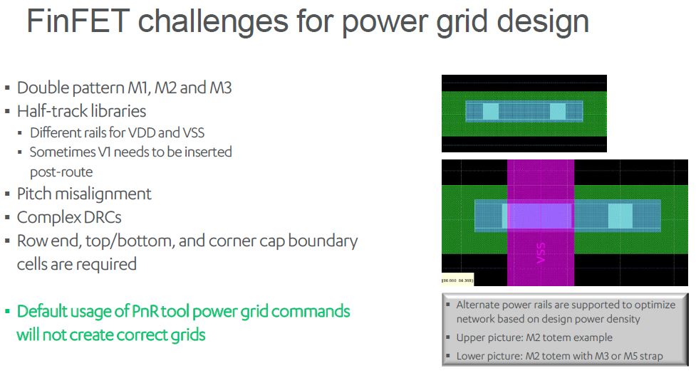
The first place most designers see the complexities of double-patterning is
in the FinFET nodes. If power planning in FinFET designs is not done right,
chips often end up with sub-optimal power grids. We at ARM have seen this
happen firsthand when engineers select the power grid over a specific block.
In some cases, the cell utilization can drop to 50-60%. But if a power grid
is carefully selected to work with the FinFET design rules and the Artisan
cell architecture, your cell utilization may be increased to over 80%; and
this is without any other design changes.
(click pic to enlarge)
|
Floorplanning in general can present challenges.  These new FinFET design
rules force new types of finishing (or boundary) cells.  Designers are
often forced to humanly read the 100's of FinFET design rules to understand
how and where to place chip finishing cells.

         ----    ----    ----    ----    ----    ----   ----

To solve this chip finishing problem for our Artisan custers, ARM created
Power Grid Architect (PGA) that uses firsthand knowledge of how to best
optimize the design rules to work with our Artisan cell architectures.  PGA
is not a standalone tool -- it is designed to work only with ARM Artisan
Physical IP and on top of your standard SNPS/CDNS/MENT/ATOP floorplanning
tools.  With PGA, chip designers can easily create power grids, insert
boundary cells and connect power gates and secondary supplies.  This lets
designers to quickly move through the floorplanning stage and onto routing;
or to spend added time exploring floorplanning options.
(click pic to enlarge)
|
During a typical floorplan session, it's possible to not notice a misplaced
power grid -- or badly sized power strap -- which can unnecessarily block
your routing channels, causing routing congestion and reduced utilization.
The end result is your design's area will increase.
Similarly, certain FinFET cell architectures may not match traditional cell
architectures in terms of power grids. A power strap centered on the cell
boundary (the traditional implementation) is not the optimal solution for
those cell architectures. Nor is inserting all vias during pre-route.
PGA automates this complexity for the designers and implements your power
grids and strap placements to be optimized for the ARM cell architectures.
(Notice how PGA made Track 4 open in the "good" layout.)
---- ---- ---- ---- ---- ---- ----
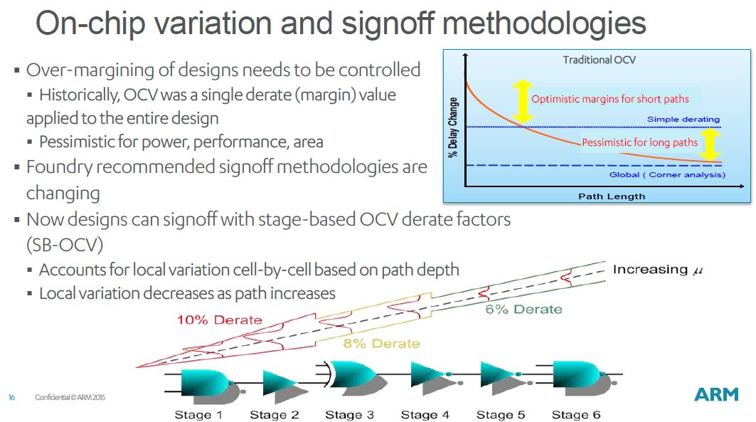
Traditionally, timing closure has been done at the extremes -- all slow and
fast devices, all minimum and maximum voltages, all coldest and hottest
temperatures. But a manufacturing process will never yield 100% at the
extremes. Not every transistor will see the same voltage. And every device
on a chip will never be at the exact same temperature. Although this
traditional signoff method ensures that your design meet the specs, it also
ensures that your chip is being over designed.

(click pic to enlarge)
|
It is safe to assume that every transistor on a die is not identical, and
every cell instance cannot be at the same voltage and temperature, nor
surrounded by uniform layout geometries.  Therefore cell delays calculated
for static timing need to be adjusted -- in other words, "derated" -- to
account for these variations.  This is called OCV, or On-Chip Variation.

         ----    ----    ----    ----    ----    ----   ----

Using a single flat OCV margin is less accurate and more conservative than
the more advanced block/path design methods -- but they work for your older
nodes.  Flat OCV margins consist of a single factor as a percentage derate
for your clock tree (and possibly your data path) delays plus a clock
uncertainty.  For example, +/- 10% of absolute clock speed.
(click pic to enlarge)
|
However, silicon is statistical in nature. When statistical methods are
applied to variation, the timing adjustments change with the length of
a data or logic path. If few devices are involved in a timing path, the
timing adjustments are larger than if there were many devices. In other
words, the statistical variation cancels out as you move along a path.
Notice how traditional OCV has optimistic margins for short paths and
pessimistic margins for long paths.
---- ---- ---- ---- ---- ---- ----
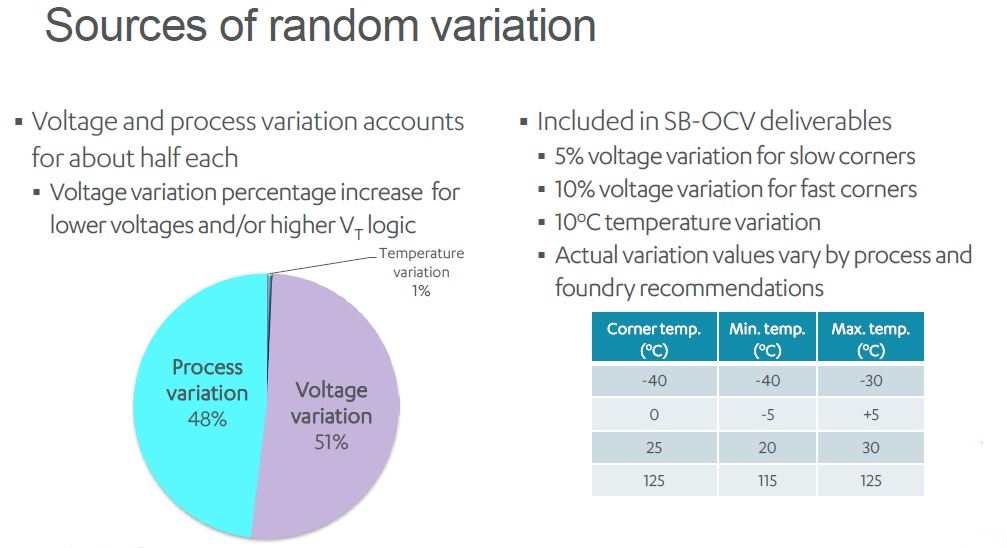
Each instance in a chip has transistors that will vary in terms of physical
parameters, supply voltage, temperature. These differences in parameters
(such as threshold voltage and line width) of a transistor can be modeled
by randomizing the parameters in the transistor models.
(click pic to enlarge)
|
Each individual transistor sees different voltages due to the instantaneous
IR-drop at its location in the power grid plus the switching activity of
nearby instances. This voltage variation can be modeled assuming a Gaussian
(or similar) distribution. Process and voltage variations each account for
about 50% (each) of total variation seen by a transistor. While temperature
variation is negligible (~1%) and systematic -- it's more per instance than
per transistor.
---- ---- ---- ---- ---- ---- ----
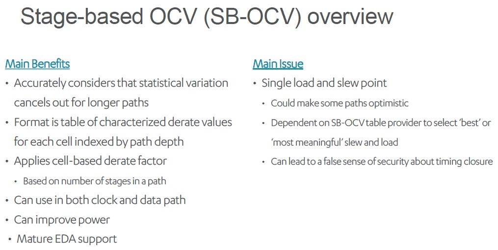
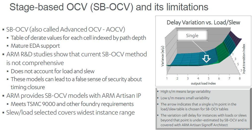
Advanced OCV (AOCV) files can contain two types of derate tables:
- Stage-based OCV (SB-OCV) derate tables indexed by path depth
and
- Location-based OCV (LOCV) derate tables indexed by distance
IP vendors characterize their SB-OCV tables using variation with in-circuit
simulators. LOCV information must be supplied by the foundry.
(click pic to enlarge)
|
Again, SB-OCV models on-chip variation using tables of derate values that
are indexed by path depth.  There are four tables that model derates for
combinations of early or late arrival of rising or falling edges.
SB-OCV derate values tend toward one as the path depth increases due to the
averaging effect.  The main challenge is that only one timing arc at one
load and slew combination can be modeled.  By applying on-chip variation
very specifically to the cell's position in a path, we remove pessimism from
the design -- but we are ignoring the effects of load and slew.

The SB-OCV approach is strongly supported by SNPS/CDNS/MENT/ATOP tools.

         ----    ----    ----    ----    ----    ----   ----

The main benefit of removing design pessimism is improving overall power,
performance and area (PPA) -- but early ARM R&D studies suggest that its
a chip's power that is primarily impacted.  Reduction in pessimism allows
for fewer hold buffers, which can result in significant dynamic power
reduction, as well as some leakage power and area reduction.  The graph
shows how slew and load affect derate values.
(click pic to enlarge)
|
The white arrow is the largest slew and load point where the least variation
is seen in the resulting derate values. You can easily move this arrow up
the curve to ensure you are assuming the worst case. But recall that the
main driver for moving to SB-OCV is to more accurately model the variation
seen by a cell -- and then apply that to a design and achieve improved PPA.
By assuming a worst case slew/load point, we are reverting to the assumption
that all transistors are under the worst case conditions for slew and load.
---- ---- ---- ---- ---- ---- ----
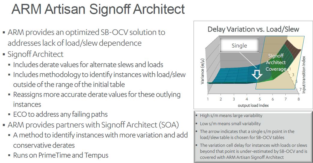
A better solution is to cover as much of the non-varying derate space with
the slew/load section, as shown with the white arrow. Our ARM R&D studies
have found that this can cover as much as 90% or more of the instances in a
given design. Then, you can avoid pessimism and address any outliers
uniquely within signoff. This is how Signoff Architect (SOA) was conceived.
(click pic to enlarge)
|
ARM developed SOA to help account for derate errors due to slew and load
not being accounted for in chip design. SOA consists of a utility and
set-up tech files; both encrypted TCL files that need license keys to use.
Signoff Architect runs equally well on SNPS PrimeTime and CDNS Tempus.
---- ---- ---- ---- ---- ---- ----
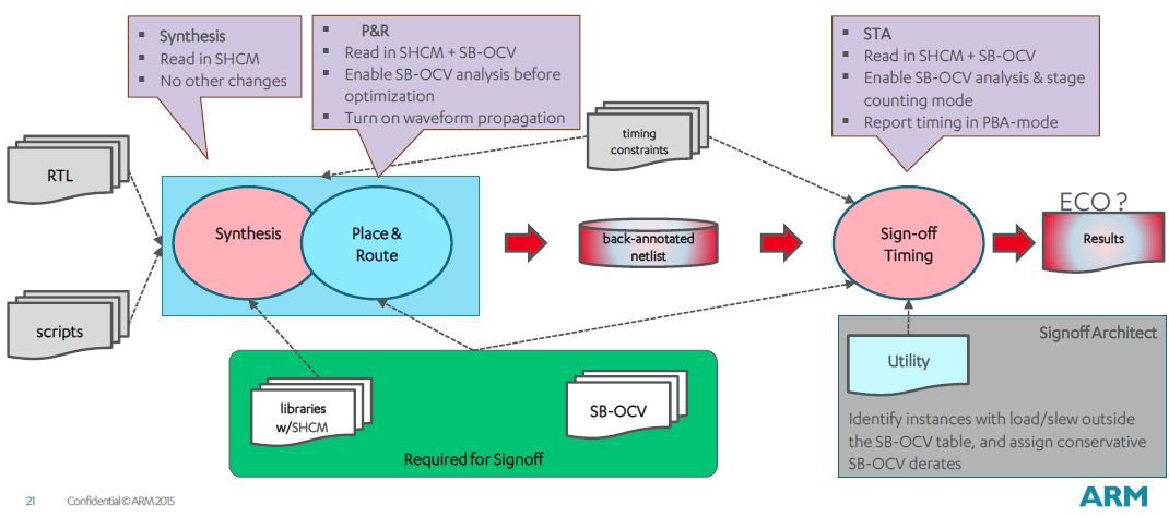
SOA is invoked during timing sign-off and it adjusts derates of instances
with loads and slews outside the bounds of the SB-OCV load-slew choice.
(click pic to enlarge)
|
ARM Power Grid Architect and Artisan Signoff Architect are not standalone
tools but work only with ARM's Logic IP Platform.  They run on top of the
standard commercial SNPS/CDNS/MENT/ATOP floorplanning/PnR/signoff tools.

    - JC Yu
      ARM Taiwan Ltd.                            Hsinchu, Taiwan
Join
Index
Next->Item
|