( ESNUG 540 Item 4 ) -------------------------------------------- [05/16/14]
Subject: Bernard Murphy's 47 quick low voltage RTL design tips (Part II)
From: [ Bernard Murphy of Atrenta ]
Hi, John,
Please read my Part I before reading this Part II here below.
- Bernard Murphy
Atrenta, Inc. San Jose, CA
---- ---- ---- ---- ---- ---- ----
A WORD ABOUT POWER STATES
You are likely to hear about sleep, light sleep, deep sleep, drowsy, dark,
dim, sneezy, happy, grumpy and so on states. OK, the last 3 aren't real but
you are going to hear about a lot of different states. Definitions aren't
hard and fast -- you may hear slightly different wordings from others.
 All of these should be viewed from the perspective of a block (rather than
low-level logic)
- Sleep -- the clock is turned off
- Deep Sleep -- and the voltage is reduced
- Deeper Sleep -- further voltage reduction
- Light Sleep -- primarily applied to power saving modes for
memories, allowing very fast recovery
- Dark -- the whole block is powered off
- Dim -- most of the block is powered off but some state is retained
(again for faster recovery)
- Drowsy -- the block is run near or below threshold voltage
It's critical to consider the tradeoffs in recovery time vs. the additional
power that may be required for recovery when considering which states to
use. You can save a lot of power by shutting off a block -- but you have to
get back to a useful state when you turn it back on -- essentially just like
you never turned it off.
That depends on the block's state and if you didn't use retention registers,
you might have to cycle through an initialization sequence to re-compute
some values -- and that can get to be slow. And if you're not careful, you
may burn as much power doing all of that as you saved in shutting down.
That said, obviously the more games you can play with switching between
these states, the more power you can save.
---- ---- ---- ---- ---- ---- ----
DESCRIBING & VERIFYING POWER INTENT
All of these techniques (apart from Vt mix and clock-gating) need to be
described in a language so they can steer implementation in RTL synthesis
and P&R and so they can be included in verification. And this all has to
be unified between verification and implementation, so you don't get a
nightmare of mismatches between stages.
To do its job, the power intent file needs to describe where you are going
to have power and voltage islands. It needs to describe where you want
level-shifter and isolation logic, where you want retention registers, and
where you will apply biasing. And you also need to define a "power state
table" (PST) -- in general you'll only allow a subset of possible
permutations of each power control. The PST table defines those power
states and the state of each control in each such state. Oddly (at least
odd to me) it does not define the state machine, only the states. How you
transition between states (and how you verify it) is left up to you.
All of these should be viewed from the perspective of a block (rather than
low-level logic)
- Sleep -- the clock is turned off
- Deep Sleep -- and the voltage is reduced
- Deeper Sleep -- further voltage reduction
- Light Sleep -- primarily applied to power saving modes for
memories, allowing very fast recovery
- Dark -- the whole block is powered off
- Dim -- most of the block is powered off but some state is retained
(again for faster recovery)
- Drowsy -- the block is run near or below threshold voltage
It's critical to consider the tradeoffs in recovery time vs. the additional
power that may be required for recovery when considering which states to
use. You can save a lot of power by shutting off a block -- but you have to
get back to a useful state when you turn it back on -- essentially just like
you never turned it off.
That depends on the block's state and if you didn't use retention registers,
you might have to cycle through an initialization sequence to re-compute
some values -- and that can get to be slow. And if you're not careful, you
may burn as much power doing all of that as you saved in shutting down.
That said, obviously the more games you can play with switching between
these states, the more power you can save.
---- ---- ---- ---- ---- ---- ----
DESCRIBING & VERIFYING POWER INTENT
All of these techniques (apart from Vt mix and clock-gating) need to be
described in a language so they can steer implementation in RTL synthesis
and P&R and so they can be included in verification. And this all has to
be unified between verification and implementation, so you don't get a
nightmare of mismatches between stages.
To do its job, the power intent file needs to describe where you are going
to have power and voltage islands. It needs to describe where you want
level-shifter and isolation logic, where you want retention registers, and
where you will apply biasing. And you also need to define a "power state
table" (PST) -- in general you'll only allow a subset of possible
permutations of each power control. The PST table defines those power
states and the state of each control in each such state. Oddly (at least
odd to me) it does not define the state machine, only the states. How you
transition between states (and how you verify it) is left up to you.
 Fig 7: A sample UPF file describing just a small subset
of what you will need to define
This being EDA, we couldn't just have one commonly agreed upon solution for
power intent -- we had to have 2 rival standards -- SNPS UPF and CDNS CPF.
UPF worked better with RTL synthesis and CPF worked better with P&R; meaning
you often needed to have both. Creating just one UPF/CPF file is hard work
and there is no way to translate between them. It looks like UPF now has
the most user traction and UPF is including features that CPF covered
that UPF did not -- so there is some hope in the near future we will only
have to deal with one standard. Nice try Cadence, but looks like you have
the Betamax of power standards. Time to move on.
There was another problem that now seems to be mostly resolved. The synth
and P&R tools change your design -- adding level shifters, power switches,
isolation logic, and retention logic -- so you are putting a lot of faith in
them to be bug-free. For a while, many customers would use the CPF/UPF
formats to describe power intent, but their engineers would do all the logic
insertion themselves for exactly this reason. I don't see as much of that
now, which suggests that bugs are less common and there are more checks and
balances between insertion and verification.
Still, creating power intent for a sizeable design is non-trivial. You're
talking thousands of lines of Tcl -- every bit as complicated as SDC and a
lot less familiar to most designers. There are a number of ways to get
through that. One is power-intent static checking (i.e. linting). Atrenta
SpyGlass Power does that for both UPF and CPF standards. Synopsys and
Cadence also have solutions.
Then there's dynamic checking. This ties power intent into simulation;
those tool you can get from SNPS/CDNS/MENT simulation vendors.
Fig 7: A sample UPF file describing just a small subset
of what you will need to define
This being EDA, we couldn't just have one commonly agreed upon solution for
power intent -- we had to have 2 rival standards -- SNPS UPF and CDNS CPF.
UPF worked better with RTL synthesis and CPF worked better with P&R; meaning
you often needed to have both. Creating just one UPF/CPF file is hard work
and there is no way to translate between them. It looks like UPF now has
the most user traction and UPF is including features that CPF covered
that UPF did not -- so there is some hope in the near future we will only
have to deal with one standard. Nice try Cadence, but looks like you have
the Betamax of power standards. Time to move on.
There was another problem that now seems to be mostly resolved. The synth
and P&R tools change your design -- adding level shifters, power switches,
isolation logic, and retention logic -- so you are putting a lot of faith in
them to be bug-free. For a while, many customers would use the CPF/UPF
formats to describe power intent, but their engineers would do all the logic
insertion themselves for exactly this reason. I don't see as much of that
now, which suggests that bugs are less common and there are more checks and
balances between insertion and verification.
Still, creating power intent for a sizeable design is non-trivial. You're
talking thousands of lines of Tcl -- every bit as complicated as SDC and a
lot less familiar to most designers. There are a number of ways to get
through that. One is power-intent static checking (i.e. linting). Atrenta
SpyGlass Power does that for both UPF and CPF standards. Synopsys and
Cadence also have solutions.
Then there's dynamic checking. This ties power intent into simulation;
those tool you can get from SNPS/CDNS/MENT simulation vendors.
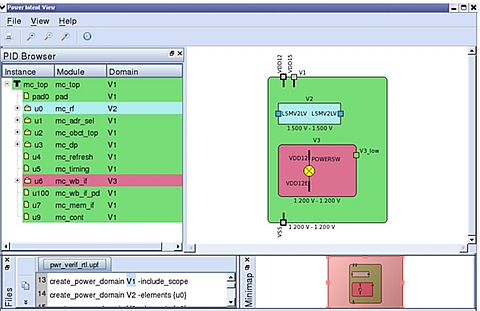 Fig 8: An example visualization of power intent. Power and
voltage islands are highlighted graphically based on
the design RTL and UPF. Visualizations like this
provide an important way to check intent which may
not be as apparent in thousands of lines of UPF.
A third method is not checking, but rather better visualization of intent.
Atrenta SpyGlass Power does this. Synopsys provides somewhat similar
viewing with its Verdi Signoff as does Cadence with its Incisive SimVision.
But remember the "checks and balances" rule of thumb -- it's best to use
implementation and verification tools from different vendors.
Fig 8: An example visualization of power intent. Power and
voltage islands are highlighted graphically based on
the design RTL and UPF. Visualizations like this
provide an important way to check intent which may
not be as apparent in thousands of lines of UPF.
A third method is not checking, but rather better visualization of intent.
Atrenta SpyGlass Power does this. Synopsys provides somewhat similar
viewing with its Verdi Signoff as does Cadence with its Incisive SimVision.
But remember the "checks and balances" rule of thumb -- it's best to use
implementation and verification tools from different vendors.
 Static checks, power-aware simulation and visualization are a starting point
in verification, but everyone agrees that these alone are not enough. Every
switchable power domain needs to be sequenced through switching between
states (that part the PST doesn't define). If you think about switching on
and off, you don't want to switch off while something is trying to access
the block, and you don't want anyone accessing the block while it's off.
You want to isolate outputs and you want to make sure retention registers
are loaded before you start powering down.
These are just some of the checks. You could imagine maybe simulating your
way through all the possibilities if you had just one domain, but if you
have ~10 or more domains each switching independently, simulation won't cut
it -- you have to go to formal. There are formal tools available like CDNS
Jasper and MENT Questa -- but they're not well UPF integrated, so setting up
the checks with them is bit of a manual task. I expect more automation will
appear over time.
Simulation plus formal works well for power switching verification because you
can decouple simulating functionality and a few power corners from formally
proving the switching behavior. This is a lot more troublesome for DVFS
and AVS. There you have changing clock frequencies so you can't formally
analyze just the neighborhood of a block -- you have to involve source and
sink blocks as well and prove behaviors in that subsystem. Certainly not
impossible but definitely a lot more work to setup with longer runs and more
bounded (incomplete) proofs.
---- ---- ---- ---- ---- ---- ----
MEMORIES & LOW POWER
Since memories consume a lot of power, there are lots of tricks which save
power in and around these IP. I mentioned one earlier that registers
driving data inputs (or outputs) for a memory can be gated under various
circumstances. Techniques to optimize power inside the memory include:
- Clock-gating or power-gating the memory decode logic and
memory sense-amps
- Voltage and frequency scaling within the memory
- Partitioning memories into smaller banks so that only the
addressed bank needs to be driven
- Divided memory word lines -- similar purpose
- Memory cache block buffering to avoid tag and data array
accesses when data needed is already in the data output
latch from the prior memory operation
All of these, if available, will be provided by your memory IP supplier.
Another big potential power saving is with external memory accesses. They
burn a lot of power driving through chip pins and PCB layers. If your DRAM
can be brought on-board, this power can be reduced dramatically. The most
obvious way to do this is through 2.5D or 3D integration. With 2.5D, your
logic die and DRAM die sit side by side on an interposer layer, connected
by metal interconnect added to the interposer using standard semiconductor
process techniques. With 3D, your DRAM die will sit on top of your logic
die, and the two are connected directly by through silicon vias (TSVs).
---- ---- ---- ---- ---- ---- ----
IP & LOW POWER
I'll focus on CPU's and GPU's, interfaces, bus fabrics and mixed-signal IP.
- Each CPU vendor offers users built-in power management options. ARM
and MIPS (Imagination) do this not only for single cores, but also
for clusters -- letting you manage power and voltage gating on a CPU
by CPU basis. Synopsys ARC and Cadence Tensilica are most likely
to be used (as far as I know) in single CPU configurations, but
they do support clock-gating and possibly dynamic voltage scaling.
- GPU's are more complicated, just by virtue of their size and large
set of features. Examples are Imagination Tech Power VR/Rogue and
ARM Mali. (Plus all the Nvidea graphics processors because they're
licensed as IP.) While these GPU's have built-in power management
similar to that of the CPU's, a practical chip also has to consider
power-gating. How that's best done is depends on the application,
so it's your problem, though I'm sure these vendors provide support
to guide you in implementing power partitioning.
- Interface logic (PCIx, USB, SATA and so on) often offer more than
one sleep state so you can fine tune power saving in idle mode.
Again, if you want to power switch, that become your job.
- Bus fabrics, both cross-bar and network on chip, get interesting
in low power designs because different parts of the bus can be in
different power states. If you power down an IP, you don't need
the part of the bus connecting to it to be "on" either. Fabric
generators from ARM, Sonics and Arteris all support this "off"
capability, but get ready for an interesting time in verification.
Now you'll have to prove not only that transactions map to correct
addresses with the correct protocol, but also that you don't have
sequencing problems for transactions as components cycle between
on and off states. This should be a formal problem, but I haven't
seen any current canned solutions to proving correctness of this.
- The number 1 problem in low power for mixed-signal IP (assuming
the IP itself works well and is appropriately shielded) is use of
incorrect level shifters between the IP and digital logic. This
most often appears as a signal which will not transition because
the voltage swing on the input to the shifter is inadequate to
switch the output. This doesn't seem to be a problem that can
easily be solved by tools or standards. Analog and digital
designers speak different languages -- it takes skilled
intermediaries to figure out if they are both talking about the
same thing when it comes to a shifter spec.
---- ---- ---- ---- ---- ---- ----
ARCHITECTURE TRICKS
Clever architecture tricks can have a huge influence on power, depending on
the chip. Here's a very small selection:
Run Fast Then Stop (RFTS) aims to optimize integrated dynamic and leakage
power. In RFTS, you have significant logic / memory shut off until some
wake-up event, and then run at high clock speed to finish quickly, and then
shut off again, as illustrated below.
Static checks, power-aware simulation and visualization are a starting point
in verification, but everyone agrees that these alone are not enough. Every
switchable power domain needs to be sequenced through switching between
states (that part the PST doesn't define). If you think about switching on
and off, you don't want to switch off while something is trying to access
the block, and you don't want anyone accessing the block while it's off.
You want to isolate outputs and you want to make sure retention registers
are loaded before you start powering down.
These are just some of the checks. You could imagine maybe simulating your
way through all the possibilities if you had just one domain, but if you
have ~10 or more domains each switching independently, simulation won't cut
it -- you have to go to formal. There are formal tools available like CDNS
Jasper and MENT Questa -- but they're not well UPF integrated, so setting up
the checks with them is bit of a manual task. I expect more automation will
appear over time.
Simulation plus formal works well for power switching verification because you
can decouple simulating functionality and a few power corners from formally
proving the switching behavior. This is a lot more troublesome for DVFS
and AVS. There you have changing clock frequencies so you can't formally
analyze just the neighborhood of a block -- you have to involve source and
sink blocks as well and prove behaviors in that subsystem. Certainly not
impossible but definitely a lot more work to setup with longer runs and more
bounded (incomplete) proofs.
---- ---- ---- ---- ---- ---- ----
MEMORIES & LOW POWER
Since memories consume a lot of power, there are lots of tricks which save
power in and around these IP. I mentioned one earlier that registers
driving data inputs (or outputs) for a memory can be gated under various
circumstances. Techniques to optimize power inside the memory include:
- Clock-gating or power-gating the memory decode logic and
memory sense-amps
- Voltage and frequency scaling within the memory
- Partitioning memories into smaller banks so that only the
addressed bank needs to be driven
- Divided memory word lines -- similar purpose
- Memory cache block buffering to avoid tag and data array
accesses when data needed is already in the data output
latch from the prior memory operation
All of these, if available, will be provided by your memory IP supplier.
Another big potential power saving is with external memory accesses. They
burn a lot of power driving through chip pins and PCB layers. If your DRAM
can be brought on-board, this power can be reduced dramatically. The most
obvious way to do this is through 2.5D or 3D integration. With 2.5D, your
logic die and DRAM die sit side by side on an interposer layer, connected
by metal interconnect added to the interposer using standard semiconductor
process techniques. With 3D, your DRAM die will sit on top of your logic
die, and the two are connected directly by through silicon vias (TSVs).
---- ---- ---- ---- ---- ---- ----
IP & LOW POWER
I'll focus on CPU's and GPU's, interfaces, bus fabrics and mixed-signal IP.
- Each CPU vendor offers users built-in power management options. ARM
and MIPS (Imagination) do this not only for single cores, but also
for clusters -- letting you manage power and voltage gating on a CPU
by CPU basis. Synopsys ARC and Cadence Tensilica are most likely
to be used (as far as I know) in single CPU configurations, but
they do support clock-gating and possibly dynamic voltage scaling.
- GPU's are more complicated, just by virtue of their size and large
set of features. Examples are Imagination Tech Power VR/Rogue and
ARM Mali. (Plus all the Nvidea graphics processors because they're
licensed as IP.) While these GPU's have built-in power management
similar to that of the CPU's, a practical chip also has to consider
power-gating. How that's best done is depends on the application,
so it's your problem, though I'm sure these vendors provide support
to guide you in implementing power partitioning.
- Interface logic (PCIx, USB, SATA and so on) often offer more than
one sleep state so you can fine tune power saving in idle mode.
Again, if you want to power switch, that become your job.
- Bus fabrics, both cross-bar and network on chip, get interesting
in low power designs because different parts of the bus can be in
different power states. If you power down an IP, you don't need
the part of the bus connecting to it to be "on" either. Fabric
generators from ARM, Sonics and Arteris all support this "off"
capability, but get ready for an interesting time in verification.
Now you'll have to prove not only that transactions map to correct
addresses with the correct protocol, but also that you don't have
sequencing problems for transactions as components cycle between
on and off states. This should be a formal problem, but I haven't
seen any current canned solutions to proving correctness of this.
- The number 1 problem in low power for mixed-signal IP (assuming
the IP itself works well and is appropriately shielded) is use of
incorrect level shifters between the IP and digital logic. This
most often appears as a signal which will not transition because
the voltage swing on the input to the shifter is inadequate to
switch the output. This doesn't seem to be a problem that can
easily be solved by tools or standards. Analog and digital
designers speak different languages -- it takes skilled
intermediaries to figure out if they are both talking about the
same thing when it comes to a shifter spec.
---- ---- ---- ---- ---- ---- ----
ARCHITECTURE TRICKS
Clever architecture tricks can have a huge influence on power, depending on
the chip. Here's a very small selection:
Run Fast Then Stop (RFTS) aims to optimize integrated dynamic and leakage
power. In RFTS, you have significant logic / memory shut off until some
wake-up event, and then run at high clock speed to finish quickly, and then
shut off again, as illustrated below.
 Fig 9: Example of tradeoff between RFTS and always-on operation.
While RFTS power consumption is higher when "on", energy
consumption integrated over time is lower for RFTS than
for always-on.
The theory is even though dynamic power is higher during the active phase,
the low leakage during the shut-off phase more than compensates. Good power
estimation is critical to making design choices here.
You can also be clever by managing leakage in SRAM's. Leakage is a function
of temperature and a memory which is frequently "on" will run at higher
temperatures. By cycling between "on" and "off" states, allowing enough
time in "off" for the memory to cool, average leakage is reduced. Knowing
when you effectively apply this technique requires software profiling on the
design to determine if the load can be managed to allow cycling.
This likely wouldn't work well for a cache (unless the corresponding CPU is
also "idle" for significant periods) but it could work well for lookup or
intermediate data tables.
---- ---- ---- ---- ---- ---- ----
ASYNCHRONOUS LOGIC
Asynchronous logic (logic without clocks) is one of those fun techniques
that makes perfect sense but has never broken through to the mainstream.
Fig 9: Example of tradeoff between RFTS and always-on operation.
While RFTS power consumption is higher when "on", energy
consumption integrated over time is lower for RFTS than
for always-on.
The theory is even though dynamic power is higher during the active phase,
the low leakage during the shut-off phase more than compensates. Good power
estimation is critical to making design choices here.
You can also be clever by managing leakage in SRAM's. Leakage is a function
of temperature and a memory which is frequently "on" will run at higher
temperatures. By cycling between "on" and "off" states, allowing enough
time in "off" for the memory to cool, average leakage is reduced. Knowing
when you effectively apply this technique requires software profiling on the
design to determine if the load can be managed to allow cycling.
This likely wouldn't work well for a cache (unless the corresponding CPU is
also "idle" for significant periods) but it could work well for lookup or
intermediate data tables.
---- ---- ---- ---- ---- ---- ----
ASYNCHRONOUS LOGIC
Asynchronous logic (logic without clocks) is one of those fun techniques
that makes perfect sense but has never broken through to the mainstream.
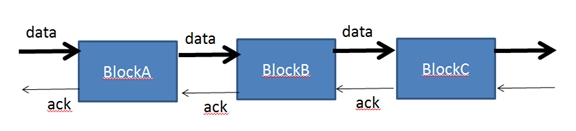 Fig 10: Basics of asynchronous logic. Modules communicate by
handshake. Within a module, logic is self-timed through
a dual-rail approach (2-bits for each desired bit).
Each stage waits for all prior bits to be ready, signaled
by encoding for each bit (00 = not ready, 01 = 0, 10 = 1,
11 = invalid).
Such logic should be intrinsically faster / lower power than clocked-logic,
but it runs counter to the synchronous training, flows and tools that are
embedded in all digital design. Changing this on a wide scale will take a
generation at least, but there could be opportunities for specialized
custom-crafted IPs, clocked around the boundaries, to make internal design
style transparent in a synchronous design flow.
One possible use of asynch logic would be for encryption IPs. Encryption
is becoming more common in many chips and can add significantly to power.
Switching to an asynchronous style could provide real differentiation in
power and performance. As an added benefit, it could make key-cracking
through Side Channel Attacks (SCA) significantly more difficult since SCA
depends on analyzing cycle-by-cycle timing, power, or EM emissions -- and
asynchronous logic doesn't have cycles.
---- ---- ---- ---- ---- ---- ----
VERILOG VS. VHDL VS. SYSTEM VERILOG VS. SYSTEMC
I have never seen any particular advantage or disadvantage between Verilog,
VHDL and System Verilog in terms of power management. Imagination GPUs are
VHDL, ARM IP is typically in Verilog, and I wouldn't be surprised to hear
that Synopsys has DW and ARC cores in all 3 languages. But, if you want to
build logic from Javascript or Fortran 77, you're on your own, baby.
Fig 10: Basics of asynchronous logic. Modules communicate by
handshake. Within a module, logic is self-timed through
a dual-rail approach (2-bits for each desired bit).
Each stage waits for all prior bits to be ready, signaled
by encoding for each bit (00 = not ready, 01 = 0, 10 = 1,
11 = invalid).
Such logic should be intrinsically faster / lower power than clocked-logic,
but it runs counter to the synchronous training, flows and tools that are
embedded in all digital design. Changing this on a wide scale will take a
generation at least, but there could be opportunities for specialized
custom-crafted IPs, clocked around the boundaries, to make internal design
style transparent in a synchronous design flow.
One possible use of asynch logic would be for encryption IPs. Encryption
is becoming more common in many chips and can add significantly to power.
Switching to an asynchronous style could provide real differentiation in
power and performance. As an added benefit, it could make key-cracking
through Side Channel Attacks (SCA) significantly more difficult since SCA
depends on analyzing cycle-by-cycle timing, power, or EM emissions -- and
asynchronous logic doesn't have cycles.
---- ---- ---- ---- ---- ---- ----
VERILOG VS. VHDL VS. SYSTEM VERILOG VS. SYSTEMC
I have never seen any particular advantage or disadvantage between Verilog,
VHDL and System Verilog in terms of power management. Imagination GPUs are
VHDL, ARM IP is typically in Verilog, and I wouldn't be surprised to hear
that Synopsys has DW and ARC cores in all 3 languages. But, if you want to
build logic from Javascript or Fortran 77, you're on your own, baby.
 Fig. 11: SystemC -- an HDL on the bleeding edge
More realistically, what about SystemC? UPF today describes power in RTL.
If you synthesize from SystemC, you will need to add your power intent after
synthesis. There is work starting in the IEEE 1801 committee to look at
extending UPF concepts up to the system level -- but I would guess any real
definition is at least a year out -- and then the tools must catch up.
---- ---- ---- ---- ---- ---- ----
POWER STATE SWITCHING -- HW & SW
Now you have a whole complicated mix of power states and controls, how do
you decide when to switch and what to switch to? Some of this can be
decided purely by the hardware. If you don't have a USB device plugged in,
that USB controller can be switched off. If the radio hasn't transmitted or
received for 10 seconds, part of the radio can be put to sleep.
Fig. 11: SystemC -- an HDL on the bleeding edge
More realistically, what about SystemC? UPF today describes power in RTL.
If you synthesize from SystemC, you will need to add your power intent after
synthesis. There is work starting in the IEEE 1801 committee to look at
extending UPF concepts up to the system level -- but I would guess any real
definition is at least a year out -- and then the tools must catch up.
---- ---- ---- ---- ---- ---- ----
POWER STATE SWITCHING -- HW & SW
Now you have a whole complicated mix of power states and controls, how do
you decide when to switch and what to switch to? Some of this can be
decided purely by the hardware. If you don't have a USB device plugged in,
that USB controller can be switched off. If the radio hasn't transmitted or
received for 10 seconds, part of the radio can be put to sleep.
 You must leave some stuff "on" to be aware when human activity is restarting
and to wake up the "sleep" logic. And there are other timer-based choices.
Think how your laptop behaves -- if nothing has happened for 10 seconds, dim
the display, then at 20 seconds turn off the display, then at 2 minutes put
most of the laptop to "sleep" (again, some logic has to remain always-on to
detect new human activity and to wake the laptop HW up.)
But the big power-saving options need OS and application-awareness. The
hardware doesn't know that you can't make a phone call and listen to MP3
audio at the same time. So many of the power control options are memory-
mapped -- and you have a combination of SW and HW inputs driving all the
state transitions in your power manager state machine.
OS power managers today make coarse optimizations through its memory-mapped
controls, but knowing how to really optimize is still a problem. However,
solutions are starting to appear.
You must leave some stuff "on" to be aware when human activity is restarting
and to wake up the "sleep" logic. And there are other timer-based choices.
Think how your laptop behaves -- if nothing has happened for 10 seconds, dim
the display, then at 20 seconds turn off the display, then at 2 minutes put
most of the laptop to "sleep" (again, some logic has to remain always-on to
detect new human activity and to wake the laptop HW up.)
But the big power-saving options need OS and application-awareness. The
hardware doesn't know that you can't make a phone call and listen to MP3
audio at the same time. So many of the power control options are memory-
mapped -- and you have a combination of SW and HW inputs driving all the
state transitions in your power manager state machine.
OS power managers today make coarse optimizations through its memory-mapped
controls, but knowing how to really optimize is still a problem. However,
solutions are starting to appear.
 Fig. 12: Aggios Concerto system power management tool
Aggios is a startup in the system power management space. Its objective
is to provide a power-aware OS (or OS component) which understands and knows
how to control all of those power switches and dials -- plus it understands
the power in each know state of your design.
From this it can provide power management based on an application-layer
understanding of system activity. You shouldn't think of this managing a
chip -- it's managing the whole board, box or whatever makes up the system.
An important part of this approach is the modeling description -- what knobs
and dials are available, how are they controlled, and what is the exact
power consumption in any given state? It's looking at measured power post-
silicon, but its approach has relevance also to design. They define this
in a format called the Unified Hardware Abstraction (UHA).
UHA is not yet another alternative to UPF and CPF. UPF/CPF describe power
intent. UHA talks about power estimation. And we're looking at it from
the software layer, meaning that those power controls need to be steerable
through those memory-mapped registers in the chip.
Aggios has donated UHA to Si2 to promote standardization in the design
community. Their motivation is obvious -- they want every chip design team
to use a UHA description which can be read into the Aggios power management
system. But UHA models could have value also during design. If we could
learn how to build such abstracted descriptions from RTL estimation, then
we could use them in emulation or TLM modeling running near top-speed. You
really could model power consumption real-time as you are running software.
---- ---- ---- ---- ---- ---- ----
NEAR- & SUB-THRESHOLD VOLTAGE OPERATION
There's quite a bit of academic work in near- and sub-threshold voltages,
and it looks like ARM may be doing something here -- but otherwise I would
consider this too exotic for most tastes.
Fig. 12: Aggios Concerto system power management tool
Aggios is a startup in the system power management space. Its objective
is to provide a power-aware OS (or OS component) which understands and knows
how to control all of those power switches and dials -- plus it understands
the power in each know state of your design.
From this it can provide power management based on an application-layer
understanding of system activity. You shouldn't think of this managing a
chip -- it's managing the whole board, box or whatever makes up the system.
An important part of this approach is the modeling description -- what knobs
and dials are available, how are they controlled, and what is the exact
power consumption in any given state? It's looking at measured power post-
silicon, but its approach has relevance also to design. They define this
in a format called the Unified Hardware Abstraction (UHA).
UHA is not yet another alternative to UPF and CPF. UPF/CPF describe power
intent. UHA talks about power estimation. And we're looking at it from
the software layer, meaning that those power controls need to be steerable
through those memory-mapped registers in the chip.
Aggios has donated UHA to Si2 to promote standardization in the design
community. Their motivation is obvious -- they want every chip design team
to use a UHA description which can be read into the Aggios power management
system. But UHA models could have value also during design. If we could
learn how to build such abstracted descriptions from RTL estimation, then
we could use them in emulation or TLM modeling running near top-speed. You
really could model power consumption real-time as you are running software.
---- ---- ---- ---- ---- ---- ----
NEAR- & SUB-THRESHOLD VOLTAGE OPERATION
There's quite a bit of academic work in near- and sub-threshold voltages,
and it looks like ARM may be doing something here -- but otherwise I would
consider this too exotic for most tastes.
 Fig 13: the familiar Ids versus Vgate curve for transistor switching.
Current seems to go to zero once below threshold Vt.
Fig 13: the familiar Ids versus Vgate curve for transistor switching.
Current seems to go to zero once below threshold Vt.
 Fig 14: expanding this same curve to a log scale shows Ids does NOT
go to zero below threshold Vt -- instead Ids falls off
exponentially. This can be used for switching.
The general idea is that if lowering voltage is good, lowering it even more
is better. The trick is what happens as you get down close to threshold or
even below threshold? Dynamic and leakage power certainly reduce -- but so
does performance -- dramatically. Think 10X slower speeds.
This could be acceptable for some chips, especially with certain Internet of
Things applications. However doing this type of design well requires very
careful characterization of transistor behavior that is not typically all
that well characterized today.
Also sub-threshold behavior is likely to be very sensitive to process and
temperature variation -- making it a very troubled design style to manage.
At most, I think we might see sub-threshold voltages emerge in certain very
specialized IP. I doubt it will become a mainstream design technique any
time soon.
- Bernard Murphy
Atrenta, Inc. San Jose, CA
---- ---- ---- ---- ---- ---- ----
Related Articles
Jim Hogan on how low energy designs will shape everyone's future
Hogan on how ultra low voltage design changes energy and power
Bernard Murphy's 47 quick low voltage RTL design tips (Part I)
Bernard Murphy's 47 quick low voltage RTL design tips (Part II)
Isadore's 28 low voltage timing sign-off & characterization tips
Trent's 12 tips on transistor and full custom low voltage design
Hogan on SNPS, CDNS, Atrenta, CLKDA, Solido as low voltage tools
Fig 14: expanding this same curve to a log scale shows Ids does NOT
go to zero below threshold Vt -- instead Ids falls off
exponentially. This can be used for switching.
The general idea is that if lowering voltage is good, lowering it even more
is better. The trick is what happens as you get down close to threshold or
even below threshold? Dynamic and leakage power certainly reduce -- but so
does performance -- dramatically. Think 10X slower speeds.
This could be acceptable for some chips, especially with certain Internet of
Things applications. However doing this type of design well requires very
careful characterization of transistor behavior that is not typically all
that well characterized today.
Also sub-threshold behavior is likely to be very sensitive to process and
temperature variation -- making it a very troubled design style to manage.
At most, I think we might see sub-threshold voltages emerge in certain very
specialized IP. I doubt it will become a mainstream design technique any
time soon.
- Bernard Murphy
Atrenta, Inc. San Jose, CA
---- ---- ---- ---- ---- ---- ----
Related Articles
Jim Hogan on how low energy designs will shape everyone's future
Hogan on how ultra low voltage design changes energy and power
Bernard Murphy's 47 quick low voltage RTL design tips (Part I)
Bernard Murphy's 47 quick low voltage RTL design tips (Part II)
Isadore's 28 low voltage timing sign-off & characterization tips
Trent's 12 tips on transistor and full custom low voltage design
Hogan on SNPS, CDNS, Atrenta, CLKDA, Solido as low voltage tools
Join
Index
Next->Item
|
|