( ESNUG 540 Item 5 ) -------------------------------------------- [05/16/14]
Subject: Isadore's 28 low voltage timing sign-off & characterization tips
> In this ESNUG post I wish to examine how the recent trend of dropping the
> on-chip voltage (VDD) -- to cut power -- ripples throughout every stage
> of chip design. Simply put:
>
> Power == (Voltage^2) / Resistance
>
> That is, as a chip's VDD drops linearly, power use drops geometrically.
>
> What follows are the nuances of how dropping to ultra-low voltages (to
> save on power, and while still maintaining performance over a range of
> temperatures) impacts how our chips are designed.
>
> - Jim Hogan
> Vista Ventures, LLC Los Gatos, CA
From: [ Isadore Katz of CLKDA ]
Hi, John,
Ultra-low voltage design creates a whole new range of problems for timing
sign-off and characterization. Many of the traditional assumptions about
delay, process variance, timing constraints, parasitic/wire load behavior,
and even the delay model itself, break down.
There's a real risk that designs which appear to pass timing sign-off at
low voltage will actually fail when in silicon. And while everyone has
their "tricks" to compensate for slow paths in silicon, almost all of them
involve detecting the violation and then dialing up the voltage and power;
which effectively defeats the whole goal. It is always better to detect
and correct these paths pre-tape out.
Fundamentally, timing for ultra-low voltage digital design looks much more
like an analog problem. Determining the real speed paths and operating
frequency below 0.7 volts requires a new look at timing and delay modeling.
---- ---- ---- ---- ---- ---- ----
4 WAYS ULTRA-LOW VOLTAGE DESIGN CAN KILL YOUR CHIP
There are 4 ways (at least) where you can miss hidden timing violations in
ultra-low voltage designs. It's essentional that you correct your timing
methodology to catch these before you end up with slow, or worse yet, bad
silicon.
1. HAVING 2X BAD DELAY CALCS
Lets start with the basics. Delay can vary by 2X across the voltage ranges
that most chips are designed at. And what's worse, at ultra-low voltage the
gap between "early" and "late" arrival (corrected for process variation) can
be huge. Underestimate that and you miss a violation. Remember, when you
check for timing violations, you are forcing one side of the path to arrive
"early" and one side of the path to arrive "late". When data arrives "late"
relative to a fast or early clock, that is a set-up violation. When data
arrives early relative to a slow/late clock, that is a hold violation.
Set-up violations force you to slow the clock frequency. Hold violations
are fatal.
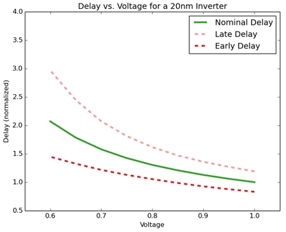 Fig 1. Shmoo plot of Delay vs. Voltage of an inverter
Above is a Shmoo plot of the delay of a basic inverter from 1 volt down to
0.6 volt at 20 nm using a load of 0.007 pF and input slew of 29 psec. It
shows how bad delay can get. (I've "normalized" the values to a delay of
1 at 1 volt to help you see how dramatic the swing can be.)
First, the nominal delay (the green line in the middle) literally doubles
from 1 volt down to 0.6 volts. That is a really big swing to try and meet
timing at different voltages, and will generate a whole range of additional
violations. That is just basics.
Second -- and this is the killer -- the gap between early and late arrival
when you add in process variation is huge. There is literally a gap of 2X
between early and late arrival.
Remedies: There are three things that can be done to fix your delay calc at
ultra-low voltages.
1. Use cells which are less sensitive to variation. There are
cells in a library which are solid at normal operating
ranges, but which simply can no longer be used at ultra-low
voltage operation, and have to be excluded.
2. Characterize everything for all voltages -- don't guess. There
are no short cuts on library characterization.
3. Use clock and data side derates. Whether it is AOCV, POCV,
SOCV or Liberty Variance Format, you need to adjust delay
for process variance at low voltage. It is simply too big
a swing to ignore.
So using real numbers, in a low-voltage design if you think you have a worse
path of 333 psec -- because of that 2X swing -- in real life it's 666 psec.
---- ---- ---- ---- ---- ---- ----
2. NON-GAUSSIAN DISTRIBUTIONS KILL YOUR DELAY CALC
Adjusting your delay calcs for process variance at ultra-low voltage has one
major complication -- the distribution is non-Gaussian. Translation: if you
assume process distribution is a "normal" or Gaussian distribution you will
get it very wrong.
The impact of process sensitivity, which was already quite noticeable once
your're below 28 nm, increases even more at low voltages. As importantly,
process variance becomes highly non-linear -- meaning its distribution is
extremely non-Gaussian -- which dramatically magnifies the impact of process
variation. Some of the allegedly adequate sigma estimation methods that
rely on sensitivities and assume a Gaussian distribution rather than real
analysis -- such as those proposed by Cadence and Synopsys -- are a joke.
Fig 1 above also showes the early and late delays (nominal +/- 3 sigma) and
illustrates the process sensitivity of the same inverter across multiple
voltages.
Fig 1. Shmoo plot of Delay vs. Voltage of an inverter
Above is a Shmoo plot of the delay of a basic inverter from 1 volt down to
0.6 volt at 20 nm using a load of 0.007 pF and input slew of 29 psec. It
shows how bad delay can get. (I've "normalized" the values to a delay of
1 at 1 volt to help you see how dramatic the swing can be.)
First, the nominal delay (the green line in the middle) literally doubles
from 1 volt down to 0.6 volts. That is a really big swing to try and meet
timing at different voltages, and will generate a whole range of additional
violations. That is just basics.
Second -- and this is the killer -- the gap between early and late arrival
when you add in process variation is huge. There is literally a gap of 2X
between early and late arrival.
Remedies: There are three things that can be done to fix your delay calc at
ultra-low voltages.
1. Use cells which are less sensitive to variation. There are
cells in a library which are solid at normal operating
ranges, but which simply can no longer be used at ultra-low
voltage operation, and have to be excluded.
2. Characterize everything for all voltages -- don't guess. There
are no short cuts on library characterization.
3. Use clock and data side derates. Whether it is AOCV, POCV,
SOCV or Liberty Variance Format, you need to adjust delay
for process variance at low voltage. It is simply too big
a swing to ignore.
So using real numbers, in a low-voltage design if you think you have a worse
path of 333 psec -- because of that 2X swing -- in real life it's 666 psec.
---- ---- ---- ---- ---- ---- ----
2. NON-GAUSSIAN DISTRIBUTIONS KILL YOUR DELAY CALC
Adjusting your delay calcs for process variance at ultra-low voltage has one
major complication -- the distribution is non-Gaussian. Translation: if you
assume process distribution is a "normal" or Gaussian distribution you will
get it very wrong.
The impact of process sensitivity, which was already quite noticeable once
your're below 28 nm, increases even more at low voltages. As importantly,
process variance becomes highly non-linear -- meaning its distribution is
extremely non-Gaussian -- which dramatically magnifies the impact of process
variation. Some of the allegedly adequate sigma estimation methods that
rely on sensitivities and assume a Gaussian distribution rather than real
analysis -- such as those proposed by Cadence and Synopsys -- are a joke.
Fig 1 above also showes the early and late delays (nominal +/- 3 sigma) and
illustrates the process sensitivity of the same inverter across multiple
voltages.
 Fig 2: Low voltage process sensitivity -- note the 0.65 V shape
Fig 2 shows how wrong it can be. When a distribution is non-Gaussian, it
is skewed. As in one side looks normal, but the other side has a very long
tail. That means that the "early" delay may be earlier, but the "late"
delay may be a lot later (or visa versa). Which means you are missing
timing violations in your chip!
Fig 2 shows the same inverter we presented in Fig 1. At 1.0 volt the
distribution looks normal. At 0.6 volt the distribution is heavily skewed
and non-Gaussian. Looking back at Fig 1, that is why the "early" delay is
1.5 (compared to a nominal delay of 2), but the late delay is 3!!!
This skew in the distribution translates directly to a skew in the "early"
and "late" timing. Underestimate this, and you miss violations.
Remedies: You have to make sure the derates for variance correct for the
skew. AOCV, POCV, SOCV and Liberty Variance Format all have the notion of
early and late derates or sigmas -- which is a natural way to correct for
non-Gaussian distribution.
Caveat: While some tools, like Variance FX, will correct for non-Gaussian
distributions, Monte Carlo SPICE systems need to be adjusted in two ways.
First, you will need to take a much larger number of samples, potentially
10,000 (and no, this is a three-sigma problem, not a six-sigma problem
which you can address with tools like Solido).
Second, you need to correctly mine the results to get early and late sigma
by actually evaluating the cumulative distribution (CDF) of the samples.
Most built-in MC SPICE reports assume a normal distribution and only report
one number.
---- ---- ---- ---- ---- ---- ----
3. BAD SLACK DUE TO BAD SET-UP/HOLD CONSTRAINTS
Equally important is the sensitivity of timing constraints when you drop to
low voltages.
Ultra-low voltage has the same impact on set-up and hold constraints as it
does on delay. They shift dramatically because of the low voltage operation
and process sensitivity. If you do not correct the constraints, you will
miscalculate slack and miss violations.
Set-up and hold constraints are the metric for slack on a path -- "positive"
slack means that a path meets timing, "negative" slack that it fails timing.
Constraints are normally associated with registers such as flip-flops or
latches, though there are also constraints for specific elements such as
clock gaters. A timing constraint determines the window when the data
and clock have to arrive for a signal value to be captured.
Again, if data arrives too late, it is a set-up violation. If it arrives
too early it is a hold violation.
Timing slack is the margin, positive or negative for the total path relative
to that window. Traditionally, constraints are characterized at the process
corners SS and FF. SS or slow nFET/slow pFET and FF or fast nFET/fast pFET,
refer to the sign-off corners that are set by a foundry, like TSMC, Samsung,
Global or UMC. If you pass timing at these corners, as measured by static
timing analysis, then the chip should function.
Fig 3 and fig 4 below capture process sensitivity for the basic set-up
constraint of a 20 nm flip-flop at 1 volt and 0.6 volts. Again these are
normalized constraint values. The average constraint is a value of 1.
Fig 2: Low voltage process sensitivity -- note the 0.65 V shape
Fig 2 shows how wrong it can be. When a distribution is non-Gaussian, it
is skewed. As in one side looks normal, but the other side has a very long
tail. That means that the "early" delay may be earlier, but the "late"
delay may be a lot later (or visa versa). Which means you are missing
timing violations in your chip!
Fig 2 shows the same inverter we presented in Fig 1. At 1.0 volt the
distribution looks normal. At 0.6 volt the distribution is heavily skewed
and non-Gaussian. Looking back at Fig 1, that is why the "early" delay is
1.5 (compared to a nominal delay of 2), but the late delay is 3!!!
This skew in the distribution translates directly to a skew in the "early"
and "late" timing. Underestimate this, and you miss violations.
Remedies: You have to make sure the derates for variance correct for the
skew. AOCV, POCV, SOCV and Liberty Variance Format all have the notion of
early and late derates or sigmas -- which is a natural way to correct for
non-Gaussian distribution.
Caveat: While some tools, like Variance FX, will correct for non-Gaussian
distributions, Monte Carlo SPICE systems need to be adjusted in two ways.
First, you will need to take a much larger number of samples, potentially
10,000 (and no, this is a three-sigma problem, not a six-sigma problem
which you can address with tools like Solido).
Second, you need to correctly mine the results to get early and late sigma
by actually evaluating the cumulative distribution (CDF) of the samples.
Most built-in MC SPICE reports assume a normal distribution and only report
one number.
---- ---- ---- ---- ---- ---- ----
3. BAD SLACK DUE TO BAD SET-UP/HOLD CONSTRAINTS
Equally important is the sensitivity of timing constraints when you drop to
low voltages.
Ultra-low voltage has the same impact on set-up and hold constraints as it
does on delay. They shift dramatically because of the low voltage operation
and process sensitivity. If you do not correct the constraints, you will
miscalculate slack and miss violations.
Set-up and hold constraints are the metric for slack on a path -- "positive"
slack means that a path meets timing, "negative" slack that it fails timing.
Constraints are normally associated with registers such as flip-flops or
latches, though there are also constraints for specific elements such as
clock gaters. A timing constraint determines the window when the data
and clock have to arrive for a signal value to be captured.
Again, if data arrives too late, it is a set-up violation. If it arrives
too early it is a hold violation.
Timing slack is the margin, positive or negative for the total path relative
to that window. Traditionally, constraints are characterized at the process
corners SS and FF. SS or slow nFET/slow pFET and FF or fast nFET/fast pFET,
refer to the sign-off corners that are set by a foundry, like TSMC, Samsung,
Global or UMC. If you pass timing at these corners, as measured by static
timing analysis, then the chip should function.
Fig 3 and fig 4 below capture process sensitivity for the basic set-up
constraint of a 20 nm flip-flop at 1 volt and 0.6 volts. Again these are
normalized constraint values. The average constraint is a value of 1.
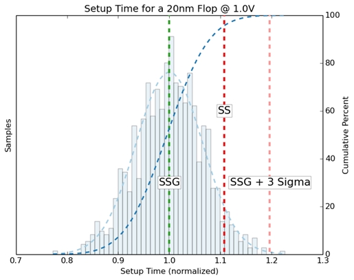 Fig 3: Set-up time process sensitivity at 1.0 V
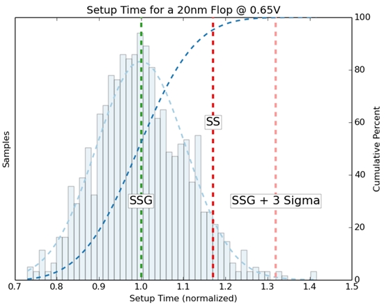 Fig 4: Set-up time process sensitivity at 0.65 V
Both of these pictures shows the probability distribution of the set-up
constraint. The bell shaped curve (though not Gaussian) is the Probability
Distribution Function (PDF).
The curve that goes up and right is Cumulative Distribution Function (CDF).
So where should the constraint be set? Traditionally, the constraint is set
at the line marked SS for the Slow-Slow corner. BUT, does that really
capture the potential impact of process variation?
Another way to set a constraint is to use a statistical value. To calculate
that, we have to use the statistical corner (called SSG) plus 3 sigma. SSG
is also provided by the foundry. It represents the corner if there is only
die-to-die variation and excludes on die variation. You add on-die or local
variation back in by using sigma.
An important note: The SS corner does NOT equal SSG-plus-3-sigma -- this is
a common myth.
Now lets look at the graphs again. The SS corner gives us a constraint of
1.1 at 1 volt. SSG-plus-3-sigma gives us a constraint of 1.2. This is much
more pessimistic.
At 0.6 volts, it gets much worse. Not only does the SS constraint shift out
to nearly 1.2, but SSG shifts out past 1.3.
Two things are work here. First, the voltage drop alone results in much
more pessimistic constraint. Second, process variance pushes the constraint
out even further.
Why? Because once again the distribution is skewed, non-Gaussian, at low
voltage. Low-voltage plus process-variation means that the safe window for
data to be captured is that much smaller.
Fig 4: Set-up time process sensitivity at 0.65 V
Both of these pictures shows the probability distribution of the set-up
constraint. The bell shaped curve (though not Gaussian) is the Probability
Distribution Function (PDF).
The curve that goes up and right is Cumulative Distribution Function (CDF).
So where should the constraint be set? Traditionally, the constraint is set
at the line marked SS for the Slow-Slow corner. BUT, does that really
capture the potential impact of process variation?
Another way to set a constraint is to use a statistical value. To calculate
that, we have to use the statistical corner (called SSG) plus 3 sigma. SSG
is also provided by the foundry. It represents the corner if there is only
die-to-die variation and excludes on die variation. You add on-die or local
variation back in by using sigma.
An important note: The SS corner does NOT equal SSG-plus-3-sigma -- this is
a common myth.
Now lets look at the graphs again. The SS corner gives us a constraint of
1.1 at 1 volt. SSG-plus-3-sigma gives us a constraint of 1.2. This is much
more pessimistic.
At 0.6 volts, it gets much worse. Not only does the SS constraint shift out
to nearly 1.2, but SSG shifts out past 1.3.
Two things are work here. First, the voltage drop alone results in much
more pessimistic constraint. Second, process variance pushes the constraint
out even further.
Why? Because once again the distribution is skewed, non-Gaussian, at low
voltage. Low-voltage plus process-variation means that the safe window for
data to be captured is that much smaller.
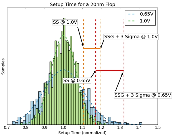 Fig 5: Set up time at 1 V versus 0.6 V
Fig 5 above overlays the distributions and constraints of the flip-flop at
1.0 and 0.6 volts. It clearly shows the disparity between the two voltage
operating points, and the increased sensitivity to process variance at the
lower voltage. And how the constraint shifts out, making it much harder
to meet timing.
This also shows that traditional SS or FF constraints, are optimistic.
Translation: if you do not adjust constraints for process variance, you
will overstate the slack on a timing path. This means missing a violation,
or ironically enough, creating one during optimization. Keep in mind that
optimization tools look for paths that have slack, and use that slack to
reduce power or fix other timing violations. But if the slack they used
is not really there, your optimizer may turn a functioning path into a
hidden timing violation.
Remedies: The traditional way to deal with optimistic set-up and hold
constraints is to add guardbands onto all of the clocks and arrival times
by using clock uncertainty and or additional delays onto clock or data.
This effectively penalizes all of the delays to reduce slack. This is a
brute force approach that impacts all paths regardless of their actual
behavior -- and for most of the designs at ultra-low voltage prevents
everything from meeting timing -- which is a bad outcome.
A new approach is to "add in" constraint uncertainty. This effectively
adjusts the constraints themselves for process variation, and removes the
risk on a situational basis. There are methodology questions that must
be addressed (like exactly how much variance to "add in"), but it is a
much more refined method.
---- ---- ---- ---- ---- ---- ----
4. BAD DELAYS DUE TO ACTIVE LOADS ON LOW VOLTAGE DESIGNS
None of the existing delay models -- CCS, ECSM -- nor the gate-level static
timing tools, PrimeTime and Tempus, address the impact of active loads
(aka Miller capacitance) posed by ultra-low voltage operation. And many
designers tell me that Miller capacitance is the biggest contributor to
delay loads below 20 nm.
Neither CCS nor ECSM understand an active load. There are workarounds that
attempt to compensate for the Miller capacitance, but their effectiveness
has diminished as the contribution of the Miller capacitance has increased.
Some people compensate by overstating the pin capacitance, but overstating
a value does not always lead to safer timing. You can end up overstating
delay on the wrong contributor -- launch clock, capture clock, data -- and
actually mask a violation.
Fig 5: Set up time at 1 V versus 0.6 V
Fig 5 above overlays the distributions and constraints of the flip-flop at
1.0 and 0.6 volts. It clearly shows the disparity between the two voltage
operating points, and the increased sensitivity to process variance at the
lower voltage. And how the constraint shifts out, making it much harder
to meet timing.
This also shows that traditional SS or FF constraints, are optimistic.
Translation: if you do not adjust constraints for process variance, you
will overstate the slack on a timing path. This means missing a violation,
or ironically enough, creating one during optimization. Keep in mind that
optimization tools look for paths that have slack, and use that slack to
reduce power or fix other timing violations. But if the slack they used
is not really there, your optimizer may turn a functioning path into a
hidden timing violation.
Remedies: The traditional way to deal with optimistic set-up and hold
constraints is to add guardbands onto all of the clocks and arrival times
by using clock uncertainty and or additional delays onto clock or data.
This effectively penalizes all of the delays to reduce slack. This is a
brute force approach that impacts all paths regardless of their actual
behavior -- and for most of the designs at ultra-low voltage prevents
everything from meeting timing -- which is a bad outcome.
A new approach is to "add in" constraint uncertainty. This effectively
adjusts the constraints themselves for process variation, and removes the
risk on a situational basis. There are methodology questions that must
be addressed (like exactly how much variance to "add in"), but it is a
much more refined method.
---- ---- ---- ---- ---- ---- ----
4. BAD DELAYS DUE TO ACTIVE LOADS ON LOW VOLTAGE DESIGNS
None of the existing delay models -- CCS, ECSM -- nor the gate-level static
timing tools, PrimeTime and Tempus, address the impact of active loads
(aka Miller capacitance) posed by ultra-low voltage operation. And many
designers tell me that Miller capacitance is the biggest contributor to
delay loads below 20 nm.
Neither CCS nor ECSM understand an active load. There are workarounds that
attempt to compensate for the Miller capacitance, but their effectiveness
has diminished as the contribution of the Miller capacitance has increased.
Some people compensate by overstating the pin capacitance, but overstating
a value does not always lead to safer timing. You can end up overstating
delay on the wrong contributor -- launch clock, capture clock, data -- and
actually mask a violation.
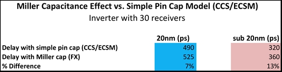 Fig 6: Miller capacitance effect vs. simple pin cap model
Fig 6 contrasts the impact of the Miller capacitance at 20 nm vs. sub-20 nm.
The error created by using a simple pin capacitance, as in CCS or ECSM,
jumps from 6% (which was already bad) to 11%. In the case of a high fanout
net (such as a clock tree), this could be fatal.
Remedies: There is none that involve CCS or ECSM. The only remedy is to
change to a new delay model.
---- ---- ---- ---- ---- ---- ----
HOW TO AVOID TIMING SURPRISES AT ULTRA-LOW VOLTAGES
Except for the "active loads" problem, many of your timing failures can be
fixed with better methodologies for calculating delay and modeling
constraints at ultra-low voltages. All of them require coming to grips
with process variation through the application of new derate standards such
as LVF, and alternative timing models, such as transistor-level timing.
1. Prepare for Liberty Variance Format (LVF). Tweaking delays to compensate
for process variance is an area of both great frustration, and continuous
innovation. The oldest way, OCV, may be unusable at ultra-low voltage.
Some have suggested doubling an already large 1.0 V value which can make
it impossible to close timing, and which again may mask violations.
AOCV is an improvement, but it has known limitations. The newly approved
Liberty Variance Format (LVF) addresses the problems in AOCV by adding
full arc/load/slew sigma data. This should provide the accuracy and
flexibility required to fix low voltage operation.
Unfortunately, neither PrimeTime nor Tempus have released full production
support for LVF -- which is a necessary precursor to foundry evaluation
and support. At DAC last year, Cadence announced they would support a
new "open" format SOCV. To date, this "open" specification has yet to
be published.
Also, generating accurate LVF tables at low voltages is non-trivial
because of the non-Gaussian distributions. As a minimum of 10,000
samples may be required if you're using traditional full Monte Carlo
sampling. Sensitivity approaches, such as those proposed by Cadence and
Synopsys, assume Gaussian behavior and even then have severe accuracy
problems.
However, SNPS and CDNS seems committed to delivering full arc/load/slew
support in their timing tools this year. With that in mind, the best
strategy may be a managed transition.
Well-designed AOCV tables for clock and data can serve as a bridge to
full LVG flows. Developing a methodology that clearly delineates
between process variance, and other margin sources takes time to develop
and implement.
2. Until there is a Liberty Standard for Constraints, there is a workaround.
Adjusting constraints for process variance is still left to the user.
Liberty has yet to propose a standard, and the only viable approach
today is to actually modify the Liberty library itself. This method
works, but it is inflexible. To modify the amount of process variance
applied to the constraint, a new library must be generated. And again,
generating accurate constraint uncertainty adjustments requires 10,000
or more samples using Monte Carlo for a non-Gaussian distribution.
---- ---- ---- ---- ---- ---- ----
THE TRANSISTOR-LEVEL TIMING REVIVAL FOR ULTRA-LOW VOLTAGES
The distinctly analog characteristics of ultra-low voltage timing is leading
to a revival of transistor level timing with tools such as Synopsys NanoTime
and CLKDA Path FX.
Transistor-level timing is no longer just the realm of the custom designer;
it addresses all of the delay and parasitic modeling concerns we have raised
in the digital world also.
- The underlying circuit simulator naturally resolves all load/slew
conditions, and can incorporate an active load by properly
connecting a receiver to the driving circuit.
- The performance issues that used to limit the application of
transistor-level timing, are largely being addressed through
improved circuit simulators, and distributed analysis.
Transistor-level timing is path-based, as opposed to PrimeTime or Tempus,
which are graph-based (though both have "path options").
Graph-based timing (GBA) evaluates all paths at once, and is faster, but
it's pessimistic and with lower accuracy.
Path-based timing only considers selected paths, and is slower, but it
eliminates pessimism -- and with transistor-level models, it can be almost
as accurate as SPICE. Most leading design teams have already shifted to
path-based sign-off precisely because of pessimism/accuracy problems with
GBA; so this issue is effectively resolved. (Process variance can be added
back in through multiple mechanisms:
- The LVF sigmas can be used so long as cells can be identified,
- Monte Carlo can be used with NanoTime, and
- Path FX has a novel analytic approach which solves for variance
with MC SPICE accuracy.
The ultimate benefit of transistor-level analysis for ultra-low voltage
timing is that it addresses all four concerns in section one with minimal
overhead. Additionally:
- It inherently addresses the accuracy issues.
- It eliminates the need to add more margin to compensate for the
limitations of delay models.
- There is little or no characterization required because transistor
approaches operate directly from the SPICE model. (Given Murphy's
Law, the probability that a foundry will change its SPICE models
just before a tape-out is painfully high.) Where CCS/ECSM models
will require weeks of characterization to determine the impact of
model change, transistor-timing can be updated literally the same
day the SPICE model arrives.
- There are multiple approaches to bringing process variance into
the transistor flow.
The traditional objection to transistor-timing, i.e. it's slow performance,
has largely been addressed relative to the potential gains in accuracy.
First, the circuit simulators used for delay calculation, such as CLKDA FX,
are all dramatically faster. Second, the use of distributed computing for
path analysis (Path FX, Tempus) keeps wall time in check (nearly linearly
in the case of Path FX).
So while it may not be a complete replacement for traditional graph-based
timing, transistor-level timing is an excellent approach to selectively
verifying critical (and potentially critical) paths, clock nets and other
mission critical parts of your design.
- Isadore Katz
CLK Design Automation Littleton, MA
---- ---- ---- ---- ---- ---- ----
Related Articles
Jim Hogan on how low energy designs will shape everyone's future
Hogan on how ultra low voltage design changes energy and power
Bernard Murphy's 47 quick low voltage RTL design tips (Part I)
Bernard Murphy's 47 quick low voltage RTL design tips (Part II)
Isadore's 28 low voltage timing sign-off & characterization tips
Trent's 12 tips on transistor and full custom low voltage design
Hogan on SNPS, CDNS, Atrenta, CLKDA, Solido as low voltage tools
Fig 6: Miller capacitance effect vs. simple pin cap model
Fig 6 contrasts the impact of the Miller capacitance at 20 nm vs. sub-20 nm.
The error created by using a simple pin capacitance, as in CCS or ECSM,
jumps from 6% (which was already bad) to 11%. In the case of a high fanout
net (such as a clock tree), this could be fatal.
Remedies: There is none that involve CCS or ECSM. The only remedy is to
change to a new delay model.
---- ---- ---- ---- ---- ---- ----
HOW TO AVOID TIMING SURPRISES AT ULTRA-LOW VOLTAGES
Except for the "active loads" problem, many of your timing failures can be
fixed with better methodologies for calculating delay and modeling
constraints at ultra-low voltages. All of them require coming to grips
with process variation through the application of new derate standards such
as LVF, and alternative timing models, such as transistor-level timing.
1. Prepare for Liberty Variance Format (LVF). Tweaking delays to compensate
for process variance is an area of both great frustration, and continuous
innovation. The oldest way, OCV, may be unusable at ultra-low voltage.
Some have suggested doubling an already large 1.0 V value which can make
it impossible to close timing, and which again may mask violations.
AOCV is an improvement, but it has known limitations. The newly approved
Liberty Variance Format (LVF) addresses the problems in AOCV by adding
full arc/load/slew sigma data. This should provide the accuracy and
flexibility required to fix low voltage operation.
Unfortunately, neither PrimeTime nor Tempus have released full production
support for LVF -- which is a necessary precursor to foundry evaluation
and support. At DAC last year, Cadence announced they would support a
new "open" format SOCV. To date, this "open" specification has yet to
be published.
Also, generating accurate LVF tables at low voltages is non-trivial
because of the non-Gaussian distributions. As a minimum of 10,000
samples may be required if you're using traditional full Monte Carlo
sampling. Sensitivity approaches, such as those proposed by Cadence and
Synopsys, assume Gaussian behavior and even then have severe accuracy
problems.
However, SNPS and CDNS seems committed to delivering full arc/load/slew
support in their timing tools this year. With that in mind, the best
strategy may be a managed transition.
Well-designed AOCV tables for clock and data can serve as a bridge to
full LVG flows. Developing a methodology that clearly delineates
between process variance, and other margin sources takes time to develop
and implement.
2. Until there is a Liberty Standard for Constraints, there is a workaround.
Adjusting constraints for process variance is still left to the user.
Liberty has yet to propose a standard, and the only viable approach
today is to actually modify the Liberty library itself. This method
works, but it is inflexible. To modify the amount of process variance
applied to the constraint, a new library must be generated. And again,
generating accurate constraint uncertainty adjustments requires 10,000
or more samples using Monte Carlo for a non-Gaussian distribution.
---- ---- ---- ---- ---- ---- ----
THE TRANSISTOR-LEVEL TIMING REVIVAL FOR ULTRA-LOW VOLTAGES
The distinctly analog characteristics of ultra-low voltage timing is leading
to a revival of transistor level timing with tools such as Synopsys NanoTime
and CLKDA Path FX.
Transistor-level timing is no longer just the realm of the custom designer;
it addresses all of the delay and parasitic modeling concerns we have raised
in the digital world also.
- The underlying circuit simulator naturally resolves all load/slew
conditions, and can incorporate an active load by properly
connecting a receiver to the driving circuit.
- The performance issues that used to limit the application of
transistor-level timing, are largely being addressed through
improved circuit simulators, and distributed analysis.
Transistor-level timing is path-based, as opposed to PrimeTime or Tempus,
which are graph-based (though both have "path options").
Graph-based timing (GBA) evaluates all paths at once, and is faster, but
it's pessimistic and with lower accuracy.
Path-based timing only considers selected paths, and is slower, but it
eliminates pessimism -- and with transistor-level models, it can be almost
as accurate as SPICE. Most leading design teams have already shifted to
path-based sign-off precisely because of pessimism/accuracy problems with
GBA; so this issue is effectively resolved. (Process variance can be added
back in through multiple mechanisms:
- The LVF sigmas can be used so long as cells can be identified,
- Monte Carlo can be used with NanoTime, and
- Path FX has a novel analytic approach which solves for variance
with MC SPICE accuracy.
The ultimate benefit of transistor-level analysis for ultra-low voltage
timing is that it addresses all four concerns in section one with minimal
overhead. Additionally:
- It inherently addresses the accuracy issues.
- It eliminates the need to add more margin to compensate for the
limitations of delay models.
- There is little or no characterization required because transistor
approaches operate directly from the SPICE model. (Given Murphy's
Law, the probability that a foundry will change its SPICE models
just before a tape-out is painfully high.) Where CCS/ECSM models
will require weeks of characterization to determine the impact of
model change, transistor-timing can be updated literally the same
day the SPICE model arrives.
- There are multiple approaches to bringing process variance into
the transistor flow.
The traditional objection to transistor-timing, i.e. it's slow performance,
has largely been addressed relative to the potential gains in accuracy.
First, the circuit simulators used for delay calculation, such as CLKDA FX,
are all dramatically faster. Second, the use of distributed computing for
path analysis (Path FX, Tempus) keeps wall time in check (nearly linearly
in the case of Path FX).
So while it may not be a complete replacement for traditional graph-based
timing, transistor-level timing is an excellent approach to selectively
verifying critical (and potentially critical) paths, clock nets and other
mission critical parts of your design.
- Isadore Katz
CLK Design Automation Littleton, MA
---- ---- ---- ---- ---- ---- ----
Related Articles
Jim Hogan on how low energy designs will shape everyone's future
Hogan on how ultra low voltage design changes energy and power
Bernard Murphy's 47 quick low voltage RTL design tips (Part I)
Bernard Murphy's 47 quick low voltage RTL design tips (Part II)
Isadore's 28 low voltage timing sign-off & characterization tips
Trent's 12 tips on transistor and full custom low voltage design
Hogan on SNPS, CDNS, Atrenta, CLKDA, Solido as low voltage tools
Join
Index
Next->Item
|
|